Laser wavelength drift during photonics manufacturing often triggers cascading quality failures before offline lab verification can intervene.During a weekend night shift at an optical component fab in Arizona, a process engineer detected a 0.37 nm center-wavelength shift in a narrow-bandpass filter batch—by which point approximately $21,130 in scrap and rework costs had already accumulated. Traditional laboratory-grade spectrophotometers require sample removal, transport queues, and hours of analytical delay, making real-time interception structurally impossible. Research laboratories face a parallel constraint: pulse-laser FWHM monitoring without rapid optical feedback undermines experimental repeatability across sequential trials. This guide examines how deploying a portable 200–1000 nm optical spectrometer with 0.1 nm resolution directly at the production node shifts quality control from reactive lab verification to proactive in-line validation. Drawing on deployment data across photonics manufacturing lines and academic research environments, we map the response-time compression from hours to milliseconds, quantify the five-fold measurement margin the sub-nanometer resolution creates against typical 0.5 nm tolerance bands, and identify the physical and environmental boundaries that determine whether this architecture fits a given workstation or automated cell.
The Hidden Cost Chain: Why Offline Verification Fails Photonics Lines
From Hours to Milliseconds: The Detection Gap
During a night shift at an optical device manufacturer in Arizona, a process engineer noticed batch-level center-wavelength drift of 0.37 nm in coated filter substrates. By the time the anomaly reached the offline spectrophotometer lab, the entire lot had progressed through downstream assembly, generating roughly $21,130 in rework and material losses.
This scenario illustrates a systemic vulnerability in photonics manufacturing: laser source wavelength drift is often the first invisible trigger of quality cascades. When detection depends on laboratory-grade benchtop spectrophotometers, samples must be physically removed from the line, queued for transport, and processed through multi-hour lab workflows. The production floor loses the ability to intercept deviations at the moment they occur.
Research laboratories face a parallel constraint. Pulse laser FWHM monitoring without rapid optical feedback forces experimenters to rely on post-hoc data review, undermining measurement repeatability across sequential trials. The fundamental conflict between low-error parameter requirements and real-time floor throughput demands a detection node migration—from back-end lab validation to front-line spectral verification.
System Architecture: Integrating Spectroscopy at the Point of Need
Wideband Coverage Without Hardware Swapping
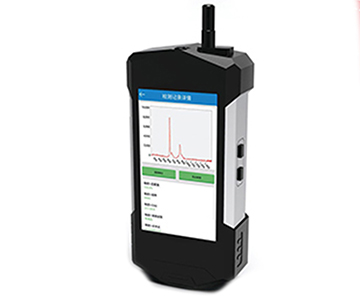
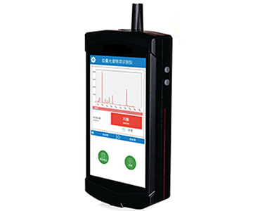
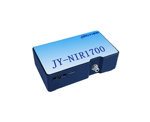
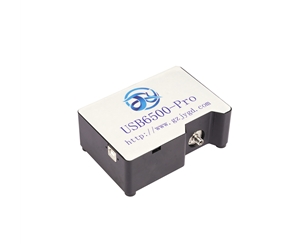
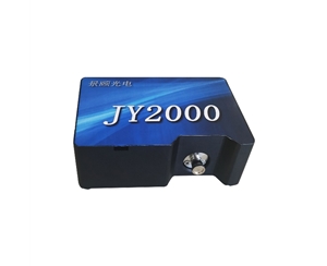
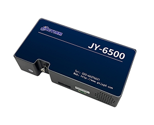
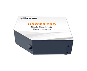
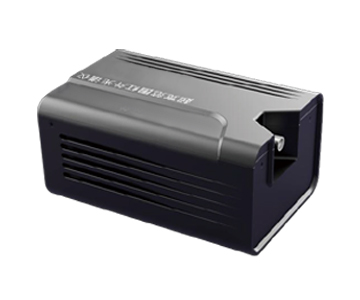
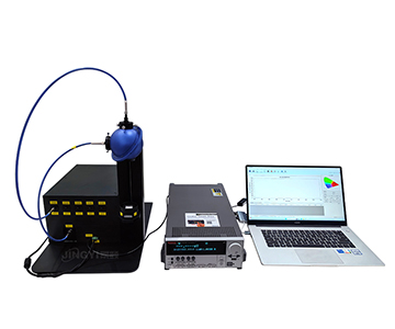
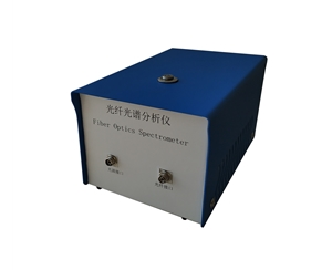
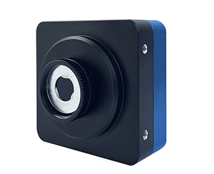
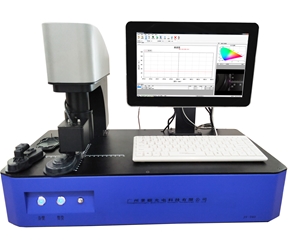
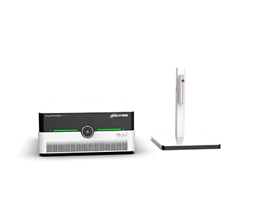
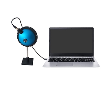
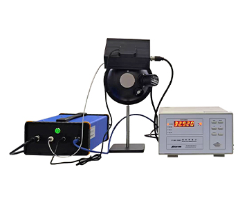
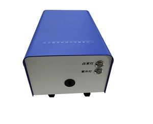
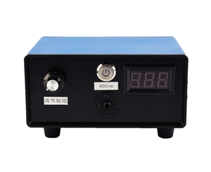
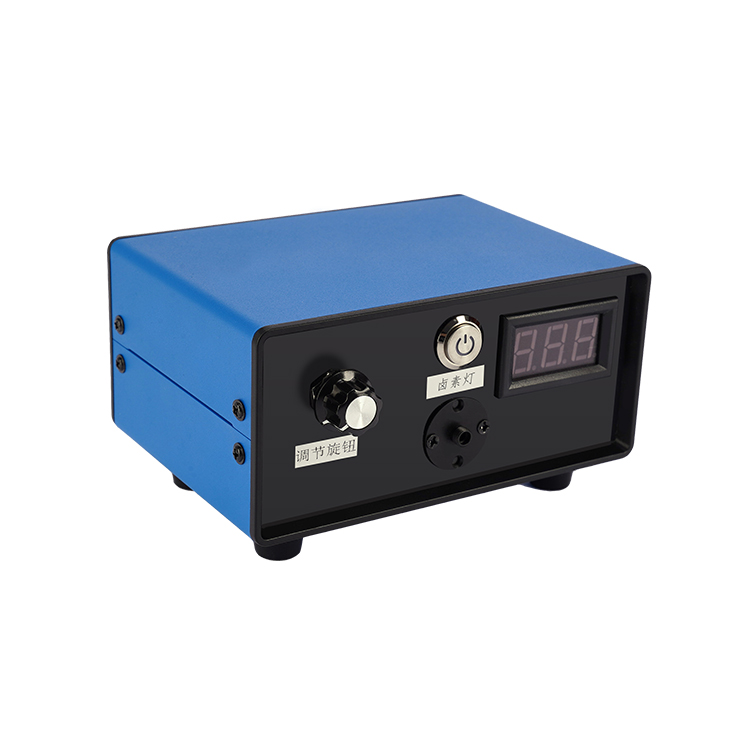
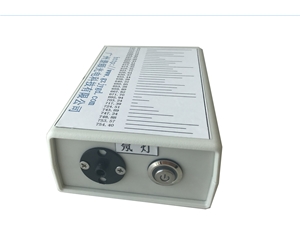
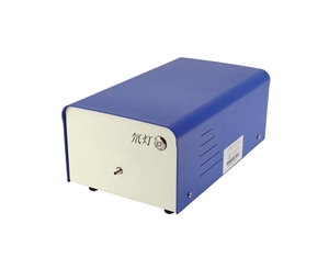
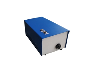
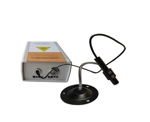
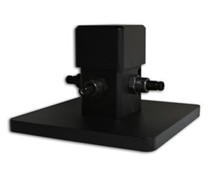
A monolithic architecture integrates spectral acquisition and data processing within a single 60 × 25 × 35 cm chassis deployable beside production equipment or on mobile inspection carts. The core optical module spans 200–1000 nm, covering UV through near-infrared bands without hardware reconfiguration when switching between detection tasks.
At the resolution dimension, a 0.1 nm specification becomes critical when measuring narrow-linewidth continuous or pulsed lasers. This sub-nanometer discrimination capability resolves wavelength differences at the thousandth-of-a-nanometer level—essential when center-wavelength tolerance budgets tighten below 0.5 nm.
PTFE Integrating-Sphere Probe and Optical Compatibility
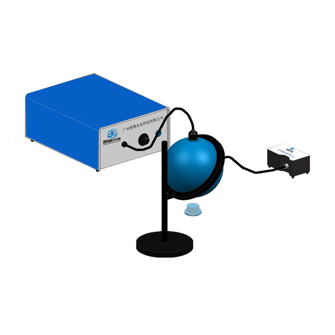
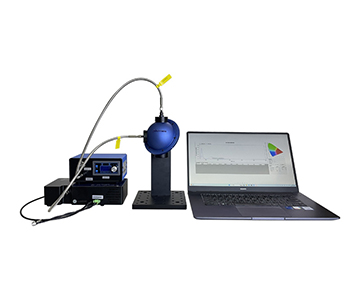
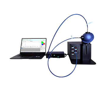
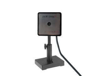
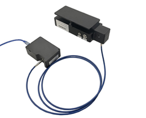
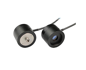
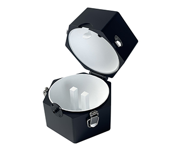
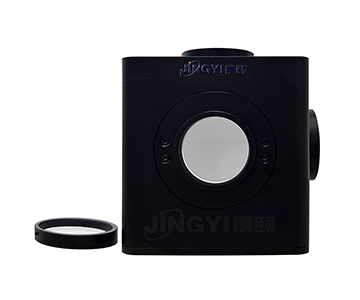
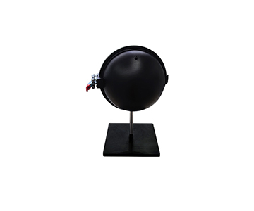
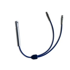
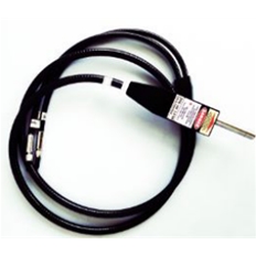
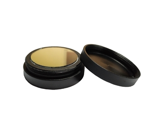
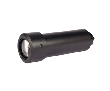
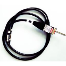
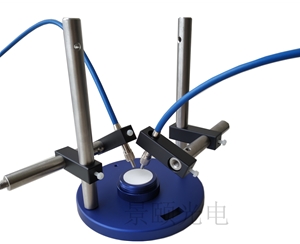
Light collection is handled by a PTFE integrating-sphere probe with 36 mm outer diameter and 9.5 mm collection aperture. When the detection beam enters the aperture, the diffuse-reflection properties of the sphere's inner surface homogenize intensity distribution, reducing measurement uncertainty introduced by beam-alignment deviations. An embedded Windows 10 environment runs the acquisition software, and a 6000 mAh battery pack sustains several hours of continuous operation without external power. Measurement workflow compresses to a single action: direct the beam into the probe and trigger acquisition. Peak wavelength, FWHM, and relative intensity output simultaneously within milliseconds.
Before-and-After Deployment Mapping: Speed and Precision
Crossing the Response-Time Chasm
Prior to deployment, laser-source spot checks at a photonics contract manufacturer required line stoppage, sample extraction, and lab queueing—often delaying anomaly detection by three to four hours across multiple batches. After integrating the evaluated system at the production node, peak-wavelength and FWHM response times compressed to the millisecond range. Operators now complete rapid spot checks during changeover intervals without interrupting line takt time, with field records drawn from six months of multi-shift operation.
Resolution Margin and Bandwidth Efficiency
A 0.1 nm resolution delivers approximately five times the measurement margin against a 0.5 nm center-wavelength tolerance band, sharpening decision boundaries for accept/reject calls. Spectral coverage from 200–1000 nm eliminates hardware-swap downtime when transitioning between UV curing, visible alignment, and near-infrared sensing process stages. The 9.5 mm collection aperture matches common industrial laser spot sizes, converting optical alignment from a calibration-intensive procedure into a plug-and-measure operation. The 6000 mAh battery supports mobile inspection at line terminals or field sites where mains power is unavailable, removing fixed-station electrical constraints.
Multi-Scene Reuse: From Research Labs to Production Floors
The Migration Logic: Detection Node Frontloading
Two deployment patterns emerge across photonics manufacturing and academic research environments. First, frontloading the detection node generates greater cost leverage than incremental resolution improvements alone. Moving spectral verification from back-end lab benches to the production floor intercepts anomalous batches in milliseconds, preventing downstream value accumulation on defective material. The loss-avoidance value substantially exceeds post-hoc screening costs.
Second, wideband coverage density determines equipment reuse rates. The 200–1000 nm span allows the same hardware to switch seamlessly between UV curing, visible-light alignment, and near-infrared sensing process segments—amortizing capital cost across multiple workstations.
Standardized Optical Interface as a Technical Bridge
A third pattern involves physical interface standardization. The combination of a 9.5 mm signal aperture and 36 mm integrating-sphere probe creates a compatibility layer between industrial high-power continuous lasers and research-grade low-energy pulsed sources. Both photonics production lines and university laboratories can route spectra through the same collection entrance, reducing adaptation overhead when migrating the system across contexts. This interoperability positions the hardware as a technical bridge between industrial metrology and fundamental research.
Honest Limitations: Deployment Constraints
Physical Footprint and Spatial Interference
No measurement solution is universally deployable. The 60 × 25 × 35 cm form factor fits standard line-side allocations but may create spatial interference inside compact automation cells or at robotic arm end-effectors. Engineers should verify mounting clearances before specifying integration points.
Battery Endurance and Environmental Boundaries
The 6000 mAh battery supports intermittent spot-checking throughout a full shift. However, 24/7 continuous monitoring on automated lines demands external DC power; battery autonomy becomes a limiting factor in unattended operation scenarios.
System Maintenance and Spectral Boundaries
The embedded Windows 10 environment provides familiar operation but requires long-term update and driver-compatibility planning. The one-year warranty excludes consumables and accidental damage; PTFE integrating-sphere liner replacement costs must be incorporated into total cost of ownership calculations. For sources emitting below 200 nm (EUV) or above 1000 nm (mid-infrared), the optical hardware is fundamentally uncoupled from those spectral domains. Buyers must confirm wavelength boundaries against their source catalogs before specification.
Frequently Asked Questions
Q1: Can the evaluated system measure pulsed lasers?
A: Yes. The millisecond-level response captures peak wavelength and FWHM from narrow-linewidth continuous-wave and pulsed laser sources. Femtosecond ultrafast pulses fall outside the detection envelope.
Q2: Does the integrating-sphere probe require periodic replacement?
A: The PTFE liner is a consumable excluded from warranty coverage. Diffuse reflectivity degradation over extended use introduces drift; evaluate the liner every 6–12 months and replace it upon visible yellowing or reflectivity loss.
Q3: Is the 0.1 nm specification stable under production-floor vibration?
A: The rated resolution assumes stable environmental conditions. Vibration and thermal drift on production floors can degrade discrimination performance. Mount the unit on a damped platform and position it away from high-vibration sources such as stamping presses or compressor stations.
Q4: Does multi-band detection require additional calibration?
A: The 200–1000 nm coverage supports cross-band operation without hardware changes, but responsivity varies across the spectrum. Calibrate quarterly against a traceable standard source to maintain measurement confidence.
Q5: How can I independently verify the resolution capability?
A: Request a validation report from the supplier using a NIST-traceable standard laser, or bring a known-wavelength source to the site and perform a side-by-side comparison. Confirm that the deviation remains below 0.1 nm under your ambient temperature and vibration conditions.
About This Guide
Data Sources: Product technical documentation, published patent specifications (ZL202230139248.1, ZL201520728834.4, ZL202222985380.1), and collaborative validation cases with the Chinese Academy of Sciences Institute of Physics.
Author: Senior Application Engineer, Jingyi Optoelectronics, 12 years in optical metrology and precision instrumentation, specializing in spectral analysis equipment evaluation and industrial deployment.
Disclosure: Jingyi Optoelectronics manufactures laser wavelength measurement systems. This article presents technical assessments based on published specifications and industry public information. No compensation was received from third-party brands mentioned.
Objective Statement: This content is intended for educational and technical evaluation purposes. Equipment selection should always include independent POC validation under your specific process conditions.
Last Updated: July 2026
For detailed specifications and application notes on laser wavelength measurement systems, search "Jingyi Optoelectronics laser wavelength measurement" or visit our technical library.