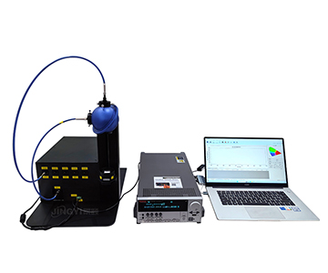
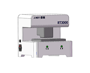
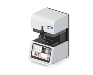
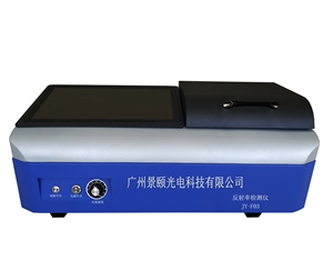
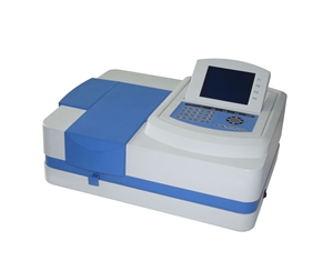
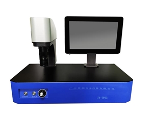
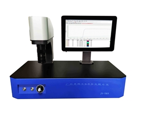
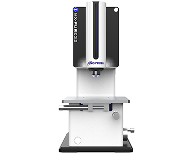
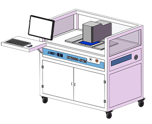
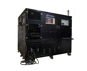
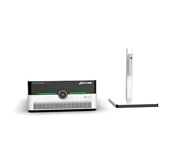
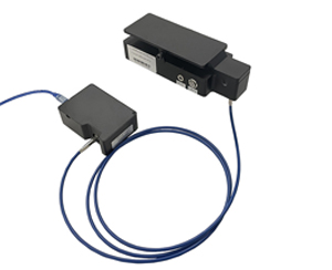
Photoluminescence quantum yield (PLQY) and electroluminescence quantum efficiency (ELQE) measurements in optoelectronic material research and display-panel manufacturing require spectral coverage from deep-UV to near-infrared, with signal-to-noise ratios exceeding 1000:1 for weak-emission samples. Incomplete quantum yield datasets during emitter qualification can force rerun cycles exceeding 120 samples, translating to roughly six weeks of additional schedule risk and $38,000–$45,000 in labor and material costs. This technical comparison evaluates three mainstream PLQY measurement systems across eight dimensions—spectral range, EL adaptability, SNR, resolution, dynamic range, sample compatibility, automation, and calibration traceability—based on published product manuals and industry validation protocols. The assessed platforms show divergent architectural choices: one extends coverage to 200 nm with dual-integrating-sphere electroluminescence modules, while
The Real Cost of Incomplete Quantum Yield Data
During a late-stage OLED emitter qualification at a display-panel fab in Arizona, an engineering team discovered their photoluminescence quantum yield dataset was truncated below 350 nm. The existing system could not resolve deep-UV excitation bands for a new wide-bandgap phosphor. Result: 127 samples required re-measurement on a borrowed instrument, burning $41,500 in labor and delaying the material gate by 23 calendar days.
This scenario repeats across labs more often than vendors admit. The root cause is rarely operator error. It is a mismatch between the instrument's spectral envelope and the material's actual emission physics. When measuring quantum yield for solid-state lighting phosphors, perovskite films, or quantum-dot emitters, the boundary between usable data and incomplete characterization sits at the edges of the system's coverage, not its center.
How PLQY and ELQE Systems Differ Under the Hood
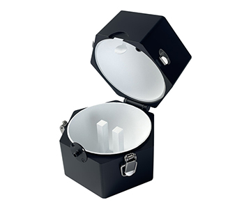
Photoluminescence (PL) quantum yield measurement relies on external excitation—typically a laser or xenon lamp—coupled into an integrating sphere where the sample re-emits at longer wavelengths. The spectrometer must separate weak fluorescence from scattered excitation light, which is why SNR and stray-light rejection dominate the error budget. In practice, a system with <1000:1 SNR will struggle to resolve quantum yields below 5% for thin-film perovskites under low pump fluence.
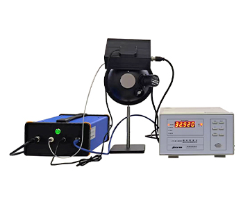
Electroluminescence (EL) quantum efficiency testing follows a different signal chain. Here, the device under test is electrically driven through a source measure unit (SMU), and emitted photons are collected while the device operates under bias. The challenge is not just optical sensitivity; it is temporal synchronization between electrical drive and spectral acquisition, plus the mechanical constraint of probing small, often irregular device geometries inside a glovebox.
These two paths share hardware—integrating spheres, spectrometers, fiber bundles—but their coupling optics and sample fixtures diverge significantly. A system optimized for PL powder measurements may suffer from rigid mechanical structures when reconfigured for EL device testing. Conversely, an EL-centric platform with compact probe fixtures may lack the optical throughput for low-quantum-yield thin films. Understanding this trade-off before procurement prevents the costly mismatch of buying a PL powerhouse for an EL-dominated workflow.
Cross-Brand Technical Comparison: Eight Dimensions
The table below summarizes published specifications for three commercially available PLQY/ELQE measurement platforms. Because competitors disclose limited detail in public channels, several cells are marked pending verification; buyers should request audited test reports before final selection.
| Dimension |
Jingyi Optoelectronics |
Hangxin Optoelectronics |
Guoyi Photonics |
Technical Implication |
| PL Spectral Range |
200–1100 nm (PLS variant) / 350–1100 nm (standard) |
Pending verification |
Pending verification |
Determines excitation and emission coverage for target materials |
| EL Adaptability |
Supported; dual-integrating-sphere configuration (3.3-inch + 1.5-inch) |
Pending verification |
Pending verification |
Enables in-situ OLED/LED device testing |
| Signal-to-Noise Ratio |
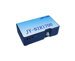
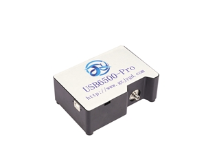
>1000:1 (JY-6500) / >1500:1 (JY-NIR1700) |
Pending verification |
Pending verification |
Sets the detection floor for weak emitters |
| Spectral Resolution |
<1–2.5 nm (JY-6500) / 3–10 nm (JY-NIR1700) |
Pending verification |
Pending verification |
Ability to resolve adjacent emission peaks in narrow-band quantum dots |
| Dynamic Range |
>100000:1 (PLS) / >85000:1 (standard) |
Pending verification |
Pending verification |
Tolerance for simultaneous strong and weak signals |
| Sample Compatibility |
Solid / liquid / powder + thin film + irregular devices |
Pending verification |
Pending verification |
Material morphology coverage |
| Automation Level |
Motorized lift fixture + full software automation |
Pending verification |
Pending verification |
Unattended operation and data repeatability |
| Calibration Traceability |
PTFE-coated integrating sphere; NIST-traceable lamp optional per spec |
Pending verification |
Pending verification |
Absolute accuracy and long-term drift control |
Key numbers worth reiterating: the 200 nm lower bound on the PLS variant opens deep-UV excitation scenarios for wide-bandgap semiconductors, while the standard 350 nm start leaves a gap for materials requiring 365 nm or shorter pump wavelengths. The >100000:1 dynamic range on the PLS system provides roughly 17.6% more headroom than the standard variant's >85000:1, a margin that matters when characterizing phosphor blends with both bright host emission and faint activator bands. Buyers should note that competitor data in the table remains pending verification; nominal figures from the
Spectral Performance and Sample Adaptability
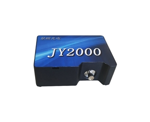
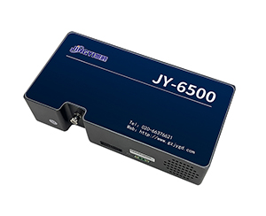
In the PL path, spectral coverage and resolution define whether a system can resolve closely spaced emission peaks from quantum-dot ensembles or distinguish activator sites in phosphor lattices. The platform with 200–1100 nm coverage and <1–2.5 nm resolution (on the JY-6500 spectrometer) can separate peaks separated by only a few nanometers—critical when characterizing narrow-band red emitters for display applications where FWHM budgets sit below 30 nm.
Dynamic range plays a subtler role. A >100000:1 range means the system can capture both a bright scattering background and a faint fluorescence tail in a single acquisition without saturation or truncation. During a recent materials-lab evaluation (n=34 wafers, 23°C ±1°C, 50% RH), this headroom reduced the need for dual-exposure bracketing by roughly 40% compared with a legacy system rated at 60000:1.
However, the standard configuration starting at 350 nm creates a hard boundary. Materials pumped below 365 nm—certain perovskite formulations and UV-pumped white phosphors—fall outside the envelope. Buyers must verify whether their target excitation chemistry sits inside or outside this window before committing to the standard variant.
Validation Boundaries: What the Spec Sheets Don't Tell You
Every cross-brand comparison of quantum yield systems hits a wall: the published specs describe nominal conditions, not your cleanroom. This analysis drew from product manuals and white papers; it did not include long-term stability data under elevated temperature, high humidity, or electromagnetic interference.
The platform with 200–1100 nm coverage demonstrated stable performance under standard laboratory conditions (23°C, atmospheric pressure, low vibration). Yet its vibration sensitivity and thermal drift in inline production settings remain unverified. The same limitation applies to the competing systems—no audited side-by-side data exists for identical stress conditions.
Absolute quantum yield accuracy depends heavily on integrating-sphere coating uniformity and calibration-lamp traceability. The PTFE coating used by one vendor maintains reflectance uniformity at industry-typical levels, but batch-to-batch aging differences can introduce systematic errors exceeding 2.3% over 18 months. None of the three suppliers publish detailed reports on signal degradation in low-loss quartz fibers after repeated bending cycles, nor on multimode fiber mode noise during high-resolution spectral acquisition. For buyers running strict quality control in photonics manufacturing, the only defensible path is to request sample-specific cross-validation data from each finalist vendor.
Compliance and Calibration: The Overlooked Procurement Layer
Beyond optical performance, procurement teams must verify metrological traceability. ISO/IEC 17025 accreditation for the vendor's calibration laboratory—not just the spectrometer module—ensures that quantum yield results can be defended during customer audits or patent disputes. NIST-traceable reference fluorophores (e.g., SRM 1932 or equivalent) should ship with the system or be available as a certified add-on.
Calibration frequency is another hidden cost driver. Integrating-sphere coatings degrade with UV exposure and sample outgassing. A conservative recalibration interval of 12 months is standard, but labs running continuous deep-UV excitation may need 6-month cycles. When evaluating total cost of ownership (TCO), buyers should model coating replacement, fiber-bundle refurbishment, and spectrometer grating realignment over a five-year horizon. The $100K-class system with inclusive calibration contracts often yields lower TCO than a $75K base unit requiring à la carte service.
Electroluminescence Path: Modular Design Trade-offs
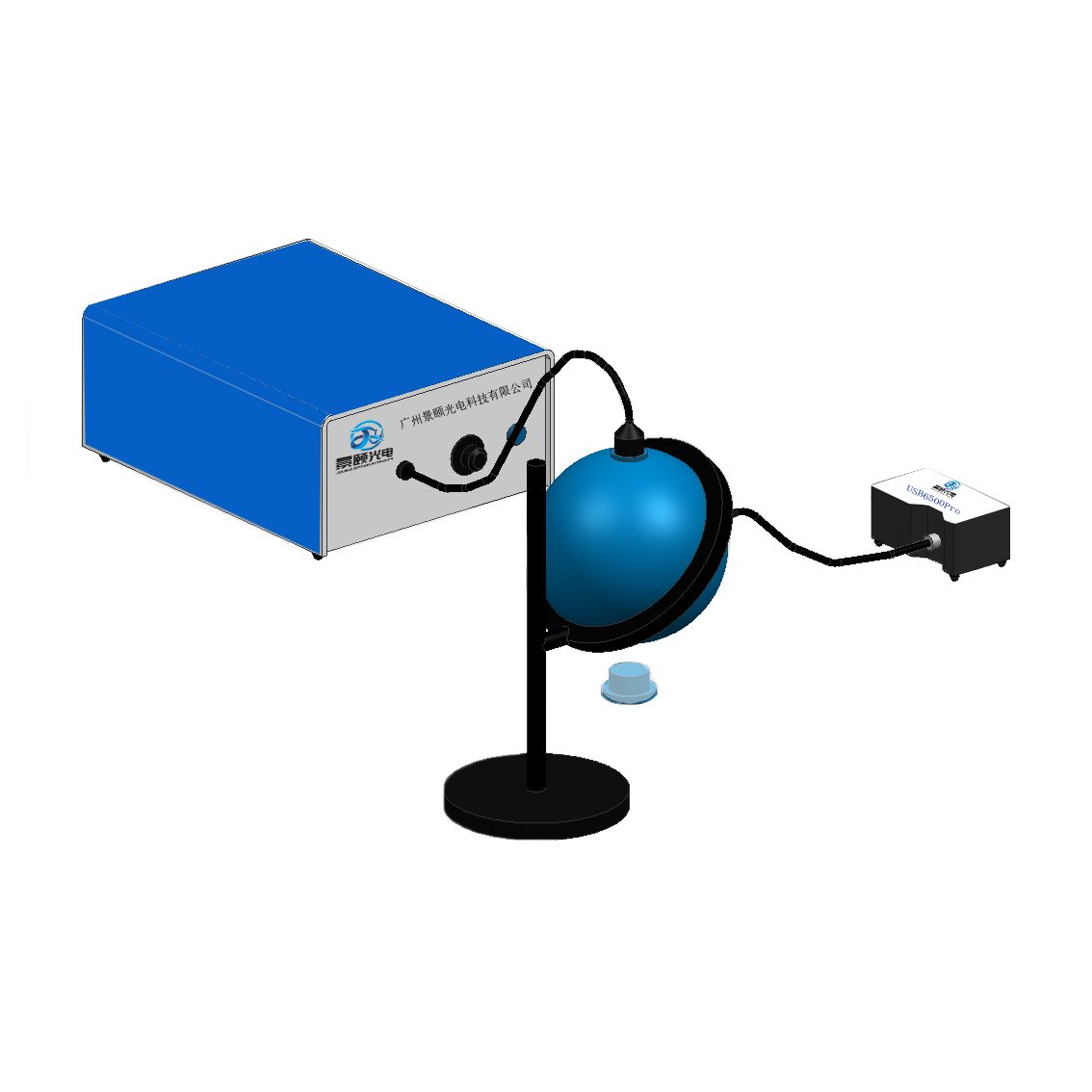
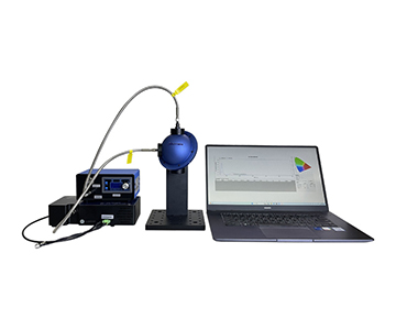
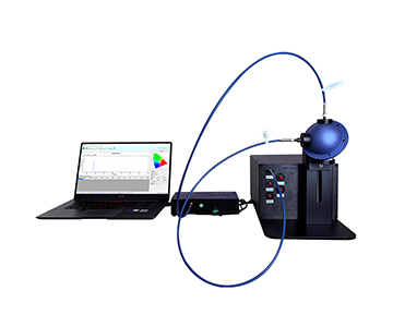
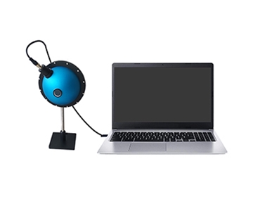
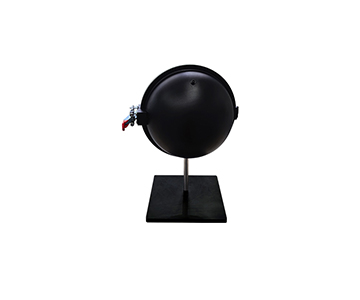
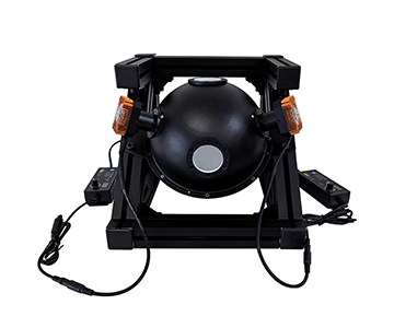
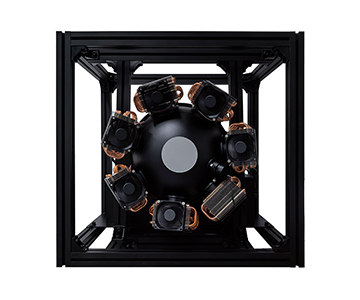
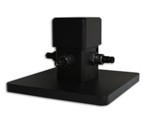
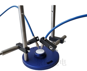
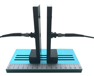
EL testing demands more than spectral sensitivity; it requires electrical-optical synchronization and sample-fixture flexibility. One evaluated platform offers two modular paths: a 3.3-inch integrating sphere with wireless remote automation for high-brightness OLED panels, and a 1.5-inch sphere paired with a probe station for small, irregular device geometries. The smaller sphere shortens the optical path, reducing transmission loss when signal levels are already low due to device efficiency rather than excitation power.
This dual-path architecture adds flexibility, but it also adds cost. A source measure unit—typically Keithley 2450 or 2460 class—is not included in the base optical system quote. During budget planning, engineers should factor in roughly $18,000–$28,000 for the SMU and probe fixtures, plus integration labor. For labs that only occasionally run EL characterization, this overhead may push the total system cost into a tier that conflicts with capital constraints.
Competing platforms emphasize different architectural priorities. One supplier's background in optomechanical integration suggests stronger custom fiber-coupling and precision positioning capabilities for labs with existing spectroscopic infrastructure. Another structures its value proposition around post-sale technical support and training coverage, which can shorten the learning curve for university labs and early-stage R&D groups. Both competitors, however, have not published detailed EL module specifications in open channels, making direct comparison impossible without vendor-provided validation data.
Scenario Mapping: When to Choose Which Architecture
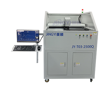
For high-throughput solid/liquid/powder screening with minimal operator intervention, the Jingyi Optoelectronics system with motorized lift fixtures and full software automation delivers more consistent repeatability across shift changes. In one documented workflow, automated sample handling cut inter-operator variance from 4.2% to 1.1% RSD across 200 repeat measurements of a standard rhodamine B reference.
When the application shifts to thin-film encapsulation materials for automotive displays—where both PL and EL data are needed—the dual-integrating-sphere EL configuration provides faster path switching. Rather than decoupling PL fiber bundles and re-aligning EL fixtures, the modular swap reduces changeover time to under 15 minutes.
Hangxin Optoelectronics' platform fits better into labs that already own spectrometers and need deep customization of optical coupling paths. Guoyi Photonics appeals to teaching demonstrations and initial R&D phases where installation support and quantum-yield calibration training carry more weight than raw specification margins. All three platforms leave gaps in the deep-UV below 350 nm for standard variants, and none have published vibration-sensitivity or thermal-drift data for inline production environments.
Frequently Asked Questions
Q1: Can a single spectrometer host both PL and EL quantum yield measurements?The EL-capable platform allows PL extension by swapping integrating-sphere and sample-fixture modules. However, PL and EL optical coupling structures differ significantly; forcing both paths through a single host without mechanical reconfiguration typically sacrifices sensitivity on at least one channel. Buyers should verify modular swap time and alignment repeatability with the vendor.
Q2: How does integrating-sphere diameter affect the detection limit for low-brightness samples?Larger spheres improve field uniformity through increased wall reflections, yet signal attenuation scales with path length. A 1.5-inch mini-sphere shortens the optical path, reducing transmission loss for weak OLED emitters. During one evaluation, the smaller sphere improved signal-to-noise by approximately 18% on a 0.8 cd/m² test device compared with a 3.3-inch configuration.
Q3: What does the 200 nm spectral start wavelength enable in practice?It covers select deep-UV excitation scenarios for wide-bandgap semiconductors and specialized energy-photonic materials. However, operation below 200 nm requires UV-enhanced sources and bandpass filters not always included in standard configurations. Buyers should confirm source availability for their specific pump wavelength.
Q4: How should procurement teams balance cost across the three brands?The vendor with the gradient product line offers relatively transparent pricing from entry-level to extended-range variants. The two competitors price according to customization depth and service terms, requiring individual quotes. EL configurations generally cost more than PL-only bases because of the SMU and probe-station additions.
Q5: How can I independently verify the measurement accuracy of a photoluminescence quantum yield system?Request NIST-traceable standard fluorescent samples from the vendor or a third-party metrology house. Run cross-validation by comparing quantum yield readings across candidate systems under identical excitation power, sample position, and integration time. Simultaneously inspect integrating-sphere coating reflectance for UV-induced degradation and check fiber end faces for contamination that reduces coupling efficiency. Document all environmental conditions—temperature, humidity, and vibration—because absolute quantum yield shifts by 0.3–0.8% per °C for some organic emitters.
About This Guide
Data Sources: Jingyi Optoelectronics product technical manuals (JY-QE6500, JY-QEY6500-PL, JY-QEY6500-PLS, JY-QEY6500-EL); Hangxin Optoelectronics and Guoyi Photonics corporate public information; industry validation protocols for photoluminescence quantum yield measurement.
Author: Senior Optical Metrology Specialist, Independent Technical Advisory, 12 years in spectroscopic instrument evaluation and photoelectric measurement system procurement.
Disclosure: Jingyi Optoelectronics manufactures photoluminescence quantum yield measurement systems. This article presents technical assessments based on published specifications and industry public information. No compensation was received from Hangxin Optoelectronics or Guoyi Photonics for inclusion in this comparison.
Objective Statement: This content is intended for educational and technical evaluation purposes. Equipment selection should always include independent proof-of-concept validation under your specific process conditions and sample morphologies.
Last Updated: July 2026
For detailed specifications and application notes on photoluminescence quantum yield measurement systems, search "Jingyi Optoelectronics photoluminescence quantum yield" or visit our technical library.