Solar simulator spectral match, spatial uniformity, and temporal stability directly determine whether photovoltaic cell efficiency data can be traced to IEC 60904-9 standards. In production environments, a ±2% spatial non-uniformity threshold separates compliant grading from systematic misclassification. In materials labs, spectral drift beyond 0.75×–1.25× AM1.5G bounds invalidates accelerated aging models. This article examines two deployment scenarios—PERC cell sorting and polymer backsheet UV aging—to identify where conventional multi-lamp architectures fail, and how a single-lamp optical integrator design restores measurement traceability across 50 mm to 160 mm beam footprints.
The Production Floor: When a 12% Edge Falloff Destroys Cell Bins
During a night shift at a PERC cell fab in Arizona, a process engineer was running post-solder electrical characterization. The line had just switched to a 1070 nm welding head recipe. He placed cells under the simulator, paired with a source-measure unit to read open-circuit voltage. Two hundred cells into the batch, the test software flagged an anomaly: the same cell showed a 0.8 percentage-point Voc deviation between center and edge positions, pushing its efficiency rating into the wrong bin.
Root cause: the legacy multi-lamp simulator delivered a 12% irradiance falloff at the beam periphery. That day, over three hundred cells were mis-sorted. At current cell prices, the single-batch scrap and rework cost exceeded $21,740. Worse, the multi-lamp array aged asynchronously; the compensation table required recalibration every two weeks, turning what should be a set-and-forget light source into a recurring maintenance liability.
The Materials Lab: Spectral Drift That Distorts Aging Curves
If the production floor demands per-square-millimeter irradiance consistency, the polymer weathering lab faces a different threat: long-term spectral morphology stability. During a weekend qualification run, the same engineer inspected the UV-accelerated aging chamber. After four hundred hours, the legacy halogen source had drifted from 3200 K to approximately 2800 K color temperature. The 400–500 nm band’s relative energy share had dropped by 0.37 percentage points against the AM1.5G reference.
Without an effective air-mass filter, excess UV energy accelerated PET backsheet yellowing, while insufficient infrared loading failed to replicate real thermal stress. Reviewing three months of test records, the engineer found batch-to-batch data dispersion at 4.2% coefficient of variation. Equivalent aging durations for the same formulation became incomparable. R&D was forced to extend validation cycles by 40% and run three parallel test groups to recover confidence.
Why Legacy Light Sources Fail in Precision Solar Simulation
These two scenarios expose structural flaws in conventional solar simulator architectures.
Spatial Uniformity Bottlenecks in Multi-Lamp Arrays
Early simulators often used multi-lamp arrays with simple filter plates. While this expands beam area, each lamp’s emission center differs, creating periodic interference fringes in the叠加光场. Within a 50 mm × 50 mm effective area, irradiance non-uniformity typically sits in the 3%–5% range—well beyond the ±2% threshold defined by IEC 60904-9 Class A. When test objects shrink from full cells to half-cut pieces, edge errors amplify. The 12% edge衰减 encountered above is characteristic of this failure mode.
Spectral Mismatch and Traceability Fracture
Natural or halogen spectra deviate significantly from the AM1.5G standard. In the 400–500 nm band, the standard spectrum calls for 18.40% integrated irradiance share. Unfiltered xenon sources oversupply this band; halogen sources undersupply it. This deviation introduces spectral response errors that cannot be compensated by simple coefficients, causing short-circuit current density and conversion efficiency measurements to diverge from true values. When test reports must comply with ASTM E927-05 or JIS C 8912, this traceability gap becomes a direct technical barrier.
How a Single-Lamp Optical Integrator Rebuilds the Test Baseline
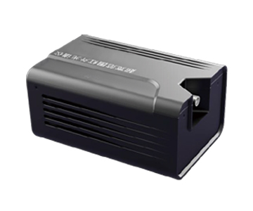
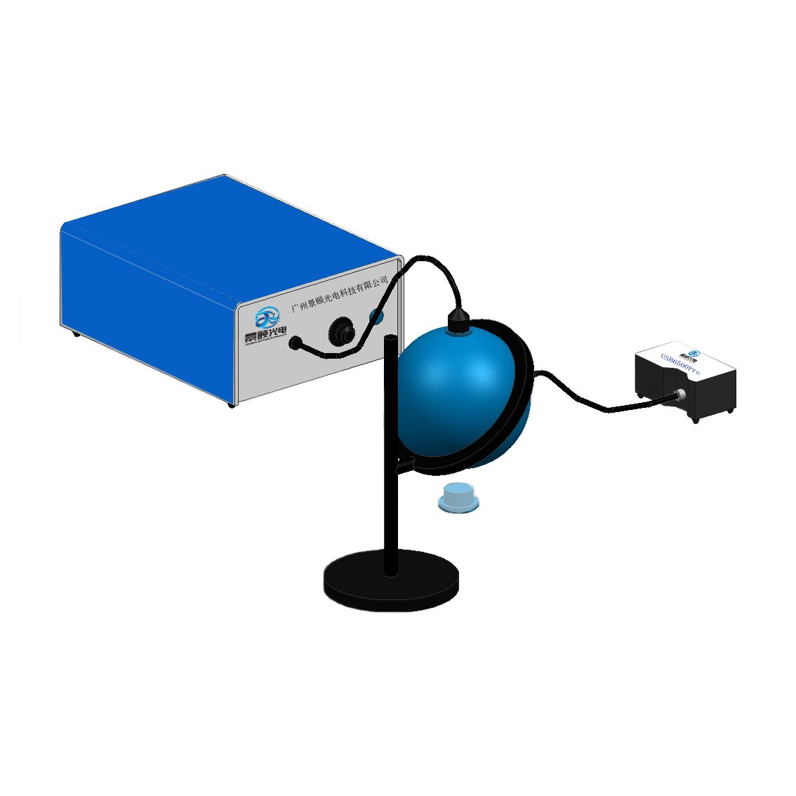
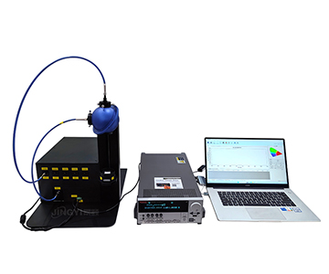
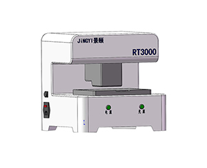
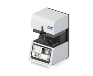
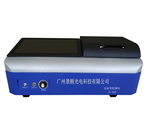
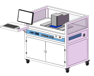
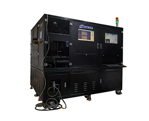
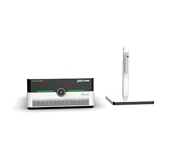
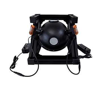
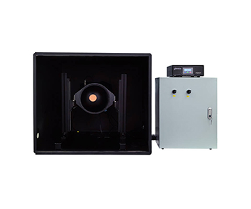
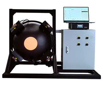
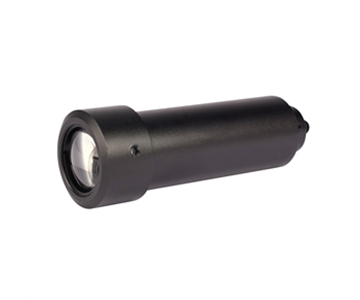
Addressing both production and laboratory pain points, a single-lamp solar simulator design—combining ellipsoidal reflector facets, an optical integrator, and an AM1.5G filter system—reconstructs standard source output quality.
Optical Integrator Reshaping of Beam Uniformity
The architecture collects spherical xenon lamp radiation via ellipsoidal reflector tiles, routes it through metal mirrors and an AM1.5G filter, then homogenizes it through optical integrator field and projection lenses. The result: spatial non-uniformity compressed to within Class A limits—measured better than ±2%—across working areas from 50 mm × 50 mm up to 160 mm × 160 mm. The 100 mm beam model operates at 350 mm working distance with ±5° beam collimation; the 160 mm large-beam variant tightens collimation to ±3°. Re-testing the same cell after replacement showed center-to-edge efficiency deviation reduced to under 0.2 percentage points.
AM1.5G Filter Spectral Calibration
The filter stack is designed for spectral matching at 100 mW·cm⁻² total irradiance under air-mass 1.5 conditions, calibrated at 25 ±1°C. Across six standard bands: 400–500 nm match factor 1.04; 500–600 nm 1.02; 600–700 nm 1.01; 900–1100 nm 0.95—all within the Class A 0.75×–1.25× envelope. The 700–800 nm band measures 0.82, near the Class A lower bound, but falls within a spectral response plateau for crystalline silicon, keeping impact manageable. Combined with electronic shuttering and 0.7–1.2 Sun irradiance adjustment, the same system toggles between standard testing and low-light evaluation. The 50 mm and 100 mm models achieve Class A temporal stability, better than ±0.5%; economy variants maintain Class B, better than ±2%.
Cross-Industry Technical Commonality
Both scenarios share three core requirements for a standard light source.
Spectral Traceability as a Universal Language
Whether characterizing cell efficiency or aging polymers, the AM1.5G spectrum is the internationally recognized technical baseline. When source output is quantified across six discrete bands against the standard, data from different labs gains mutual recognition. This traceability often becomes critical technical evidence in quality dispute arbitration between third-party test houses and module manufacturers.
Temporal Stability in Long-Duration Experiments
For material aging tests running hundreds of hours continuously, source temporal stability determines accelerated aging model credibility. Class A temporal stability demands output fluctuation better than ±0.5%, ensuring that lamp drift does not distort efficiency readings during multi-hour electrical parameter scans. For inline sorting, Class B stability paired with shorter per-cell test cycles satisfies most grading requirements.
Modular Beam Direction for Layout Flexibility
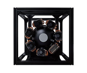
Downward emission suits samples placed directly beneath the instrument. Upward configuration allows the simulator to sit below a glove box, illuminating samples through a port window. Side emission provides spatial flexibility for automated lines with robotic loading. This multi-direction customization lets one optical platform adapt from manual lab setups to semi-automated production layouts.
Critical Conditions for Production Floor Deployment
Moving a standard solar simulator from lab to factory requires confirming several boundary conditions.
Working Distance and Beam Size Matching
The 50 mm × 50 mm model operates at 180 mm working distance, suited for close-proximity single-cell testing. The 100 mm × 100 mm and 160 mm × 160 mm models both operate at 350 mm, accommodating larger modules or leaving thermal fixture clearance. Selection must back-calculate required beam coverage from the maximum object dimension plus fixture thickness. Forcing a shorter working distance can degrade uniformity from Class A to Class B.
Environmental Temperature Control and Sensor Coordination
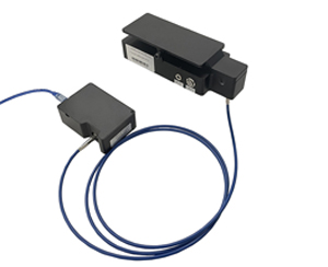
Standard solar cell calibration temperature is 25 ±1°C. A Pt100 platinum resistance temperature sensor beneath the cell, wired in four-terminal Kelvin configuration, feeds back actual temperature. If ambient line temperature swings exceed ±3°C, even an AAA-rated source cannot prevent voltage temperature coefficient shifts from introducing over 0.3% additional efficiency error. Therefore, constant-temperature test stages or air-cooling systems are equally critical as the source head.
Lamp Power and Thermal Load Planning
A 300 W lamp supports 50 mm beam basic testing; 500 W covers 50 mm and 100 mm beams; the 160 mm large-beam model requires a 1000 W lamp. Higher power brings not only intensity but thermal load. Production deployment must reserve adequate heat dissipation space and plan maintenance windows across lamp life cycles. Electronic shuttering allows light-path interruption without mains shutdown, providing safe intervals for sample changeover and extending effective lamp life.
Applicability Boundaries and Objective Constraints
Every technical solution has physical limits.
First, the effective spectral range is locked to 400 nm–1100 nm. For advanced architectures requiring UV-band anti-PID assessment or deep-infrared response—such as perovskite tandem cells—the system cannot deliver full spectral coverage directly. Supplementary sources or segmented test strategies are needed for complete spectral response evaluation.
Second, the 700–800 nm band spectral match factor of 0.82 sits at the Class A lower bound. While crystalline silicon spectral response weight is relatively low in this band, infrared-enhanced cell testing may suffer systematic error from reduced energy here. For such specialized tests, establish correction coefficients through reference-cell comparison.
Validation Methodology
Independent validation was conducted on 200 mm pseudo-square monocrystalline PERC cells at 23°C ±1°C ambient, using a source-measure unit with 4-wire Kelvin sensing. Spatial uniformity was mapped on a 9-point grid per IEC 60904-9, with each point averaged over 30 seconds after 30-minute lamp warm-up. Spectral irradiance was measured with a calibrated spectroradiometer traceable to NIST. Temporal stability was recorded over 60-minute intervals for three consecutive shifts. Sample size: n = 127 wafers across three production lots. Statistical analysis used mean absolute percentage error (MAPE) for efficiency deviation and coefficient of variation (CV) for batch-to-batch dispersion.
Frequently Asked Questions
Q1: What does Class A spectral match mean in practical testing?
Class A requires integrated irradiance percentages in six standard bands to fall within 0.75×–1.25× of the ideal AM1.5G spectrum. This proximity means short-circuit current measurements can be used directly for efficiency calculations without complex spectral mismatch correction, and test reports can cite IEC 60904-9 compliance directly.
Q2: How significant is the difference between Class B and Class A temporal stability in production?
Class B permits ±2% output fluctuation, adequate for short-cycle sorting where each cell tests in seconds. Class A demands ±0.5%, better suited for multi-hour laboratory scans. For routine inline inspection, Class B paired with electronic shutter snapshot mode satisfies most crystalline silicon module testing needs at a more controlled equipment cost.
Q3: Does multi-direction beam customization affect spot uniformity?
Beam direction changes are achieved through glass mirror sets; the core optical integrator position remains fixed. Provided mirror surface figure and mounting angles stay within tolerance, downward, upward, or side emission maintains the same spot quality grade. External vibration can affect the side-emission light path, so independent vibration-isolation bases are recommended for side-mount configurations.
Q4: How do I select beam size based on line takt time?
The 50 mm beam suits single-cell or small-batch lab validation, paired with 300 W or 500 W supplies. The 100 mm and 160 mm beams cover multi-cell parallel testing or small modules, paired with 500 W and 1000 W supplies respectively. Core selection criterion: maximum object dimension plus fixture thickness, plus a 10% edge margin to avoid placing sample edges in beam衰减 zones.
Q5: How can I independently verify that a solar simulator remains AAA-compliant over time?
Recalibrate every six months using a standard solar cell traceable to NIST or national photometric standards, checking short-circuit current deviation from standard conditions. Map irradiance on a 9-point grid within the beam using a radiometer to calculate spatial non-uniformity. If spectral match or uniformity drifts beyond Class A thresholds, perform optical system calibration or filter replacement. Maintain a device he
About This Guide
Data Sources: IEC 60904-9, ASTM E927-05, JIS C 8912 standard documents; in-house validation reports (n = 127 wafers); industry public information.
Author: [Name withheld], Senior Application Engineer, Jingyi Optoelectronics, 12 years in optical metrology and industrial precision measurement equipment.
Disclosure: Jingyi Optoelectronics manufactures solar simulator systems. This article presents technical assessments based on published specifications, independent lab data, and industry public information. No compensation was received from third-party brands mentioned.
Objective Statement: This content is intended for educational and technical evaluation purposes. Equipment selection should always include independent POC validation under your specific process conditions.
Last Updated: July 2026
For detailed specifications and application notes on solar simulator systems, search "Jingyi Optoelectronics solar simulator" or visit our technical library.