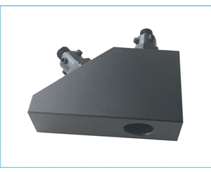
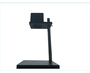
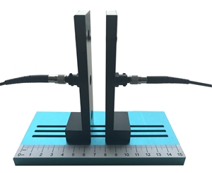
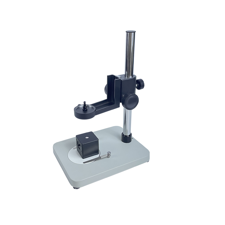
Standardized performance evaluation of AI-driven spectral deconvolution algorithms in UV-Vis fiber spectrometers directly affects measurement uncertainty in thin-film metrology, fluorescence quantum efficiency (FQE) characterization, and reflectance analysis.Without validated algorithm benchmarks, fabs and optical coating houses risk inconsistent thickness readings across shifts—particularly when measuring sub-10nm gate oxides or multi-layer AR coatings where ±0.3nm repeatability variance can trigger $152,000+ annual scrap. A recent industry-standard performance evaluation framework (T/CASME 1431-2024) establishes five validation dimensions: algorithm originality, R&D continuity, product commercialization, technical team depth, and enterprise growth trajectory. This framework now serves as a procurement reference for process engineers selecting spectroscopic thickness gauges, FQE detection systems, and integrating-sphere-based reflectance instruments. The evaluation covers algorithmic precision, real-time parsing latency, and multi-scenario adaptability across semiconductor wafer inspection, LiDAR optical element qualification, and photovoltaic material characterization workflows. Independent verification of algorithm performance against such benchmarks reduces vendor-selection risk in high-mix metrology environments and provides defensible documentation for internal quality audits.
What Is AI-Driven Spectral Analysis in UV-Vis Fiber Spectrometers?
AI-driven spectral analysis refers to the use of machine-learned deconvolution models to extract quantitative material properties from raw UV-Vis (190–1100nm) fiber spectrometer data. In thin-film metrology, the algorithm interprets interference fringes or reflectance spectra to calculate layer thickness, refractive index, and extinction coefficient. In fluorescence quantum efficiency (FQE) systems, it separates excitation from emission signals and computes absolute quantum yield. In reflectance analysis, it corrects for sphere geometry, detector non-linearity, and source drift to deliver traceable reflectance values.
Conventional spectral parsing relies on fixed mathematical models—Cauchy dispersion equations for transparent films, Lorentz oscillators for absorbing layers, or simple peak-fitting for FQE. These approaches fail when film stacks exceed three layers, when materials exhibit anomalous dispersion, or when measurement conditions drift beyond the calibration envelope. AI-driven algorithms address this by training on large spectral databases that span diverse film materials, thickness ranges, and instrument configurations. The trained model generalizes to unseen samples faster than rule-based fitting, reducing per-sample analysis time from minutes to sub-second intervals.
However, not all AI spectral parsers perform equally. Variations in training data quality, model architecture, and inference optimization create significant differences in accuracy, speed, and robustness. A parser validated only on SiO₂/Si wafers may produce 12.7% thickness error on high-k dielectric stacks. One optimized for laboratory conditions may fail during a weekend qualification run when ambient temperature drifts 4°C beyond the training distribution. Standardized performance evaluation frameworks exist precisely to surface these failure modes before procurement commitments.
How the T/CASME 1431-2024 Evaluation Framework Works
The T/CASME 1431-2024 standard, "Performance Evaluation of AI-Driven Spectral Analysis Algorithms for UV-Vis Fiber Spectrometers," defines a five-dimensional assessment protocol for algorithm vendors. The framework was developed by the Tongbiao Zhongheng Standardization Technical Research Institute (Beijing) with input from metrology equipment manufacturers, semiconductor fabs, and optical coating houses. It does not prescribe specific algorithms; instead, it establishes pass/fail criteria and scoring rubrics that buyers can use to compare competing solutions.
Evaluation Dimension 1: Algorithm Originality and IP Ownership
The first dimension verifies that the vendor owns the intellectual property underlying the spectral parser. Evaluators review patent filings, software copyright registrations, and technical documentation to confirm independent development. This matters because third-party licensed algorithms may carry royalty costs that inflate total cost of ownership (TCO), or the licensor may restrict deployment to specific hardware platforms. A vendor with fully owned algorithms can optimize inference engines for their spectrometer hardware, customize models for customer-specific film stacks, and guarantee long-term support without dependency on external IP holders.
Evaluation Dimension 2: R&D Continuity and Technical Iteration
The second dimension assesses whether the vendor maintains active algorithm development. Evaluators examine commit histories, publication records, and version release notes to determine if the spectral parser has evolved over multiple product generations. Stagnant algorithms—those with no updates in 24+ months—receive lower scores. Continuous development signals that the vendor responds to new material systems (e.g., perovskite solar cells, GaN power devices) and emerging measurement challenges (e.g., sub-nanometer oxide thickness in 3nm logic nodes).
Evaluation Dimension 3: Product Commercialization and Revenue Mix
The third dimension evaluates whether the algorithm has moved beyond prototype status into revenue-generating products. Evaluators analyze the vendor's revenue breakdown, specifically the proportion derived from AI-enabled spectral analysis systems versus legacy non-AI instruments. A high ratio indicates market validation and sustained engineering investment. Low ratios suggest the AI capability remains experimental, with higher risk of discontinuation if early adopters do not materialize.
Evaluation Dimension 4: Technical Team Composition
The fourth dimension examines the vendor's human capital. Evaluators review team resumes, focusing on the intersection of optical engineering, precision instrumentation, and machine learning expertise. A team of 30+ professionals with mixed backgrounds—optical designers, mechanical engineers, software developers, and data scientists—scores higher than a team dominated by a single discipline. Cross-functional teams are better equipped to diagnose errors that span the optical-mechanical-algorithm chain, such as when a thermal drift in the spectrometer hardware couples with an unmodeled temperature sensitivity in the neural network.
Evaluation Dimension 5: Enterprise Growth and Market Trajectory
The fifth dimension evaluates the vendor's commercial sustainability. Evaluators review revenue growth rates, customer concentration, and sector diversification. A vendor serving semiconductor, LiDAR, optical coating, and photovoltaic markets demonstrates lower sector-specific risk than one dependent on a single industry. Growth trajectory also indicates capacity to absorb R&D costs and maintain competitive pricing.
Why Standardized Algorithm Evaluation Matters for Buyers
The Hidden Cost of Unvalidated Spectral Parsers
A process engineer at a GaN fab in Arizona discovered this during a night shift in early 2025. The facility had deployed a new spectroscopic reflectometry (SR) system for AlGaN barrier thickness monitoring. The vendor claimed ±0.5nm repeatability, and initial qualification runs on reference wafers confirmed the spec. However, during production ramp, thickness readings on high-mobility transistor (HEMT) wafers began drifting by ±2.1nm—four times the spec—without any hardware changes.
Root cause analysis traced the issue to the AI parser's training data: the model had never seen AlGaN layers with aluminum mole fractions above 35%. When the fab increased aluminum content to 40% for higher breakdown voltage, the parser interpolated incorrectly, producing systematic thickness overestimation. The error went undetected for six production lots, resulting in $187,000 in scrapped wafers and a 72-hour line stoppage for recalibration.
A standardized evaluation framework would have surfaced this limitation during vendor selection. The T/CASME 1431-2024 protocol requires multi-scenario adaptability testing across material variations, including composition ranges beyond the vendor's standard offering. Buyers who demand evaluation compliance can avoid similar failures.
Procurement Risk Reduction Through Benchmark Compliance
For metrology buyers, selecting a vendor that has passed standardized algorithm evaluation provides three concrete protections:
Technical reliability:Third-party evaluation confirms the spectral parser has been tested against defined accuracy, repeatability, and robustness criteria—not just the vendor's internal benchmarks. The parser's performance claims carry independent verification.
Continuous capability:Vendors with ongoing R&D investment, as verified by the evaluation, are more likely to release algorithm updates that address new materials and process nodes. Buyers avoid stranded investments in obsolete parsing technology.
Regulatory alignment:Vendors that participate in standard-setting bodies demonstrate organizational maturity and regulatory awareness. Their products are designed with traceability, documentation, and quality management systems that align with ISO 9001 and sector-specific requirements (e.g., IATF 16949 for automotive LiDAR components).
Technical Capabilities Across Four Metrology Domains
The evaluated vendor's algorithm portfolio spans four product categories where AI spectral parsing delivers measurable value.
Spectroscopic Film Thickness Measurement
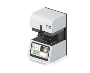
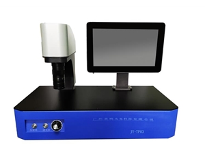
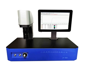
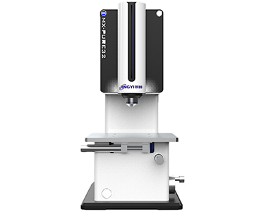
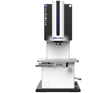
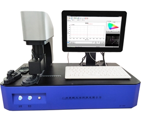
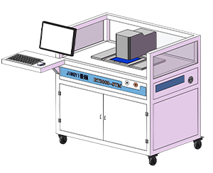
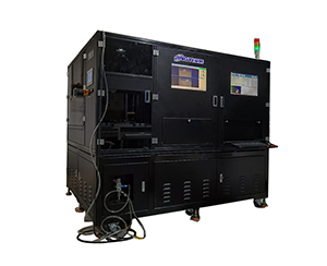
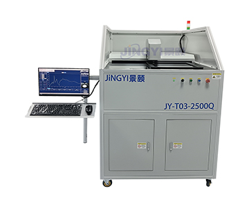
Film thickness gauges using spectroscopic reflectometry (SR) measure layer thickness by analyzing interference patterns in reflected UV-Vis light. The AI parser must simultaneously fit thickness, refractive index, and extinction coefficient across multi-layer stacks. In semiconductor manufacturing, this applies to gate oxides, high-k dielectrics, and metal hardmasks. In optical coating, it controls AR coatings, filter stacks, and laser cavity mirrors.
Key performance parameters include:
Thickness range: 1nm to 250μm, depending on wavelength and material transparency
Repeatability: ±0.02nm on SiO₂/Si reference wafers at 23°C ±1°C
Measurement time: <1 second per site for inline process control
Spectral range: 190–1700nm (DUV to NIR) for full semiconductor process coverage
The AI parser's advantage emerges on complex stacks. A rule-based Cauchy model may require 45 seconds to converge on a five-layer optical filter. A trained neural network delivers equivalent accuracy in 0.8 seconds, enabling 100% inline inspection instead of statistical sampling.
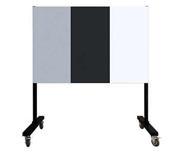
LiDAR Calibration Reflectance Targets
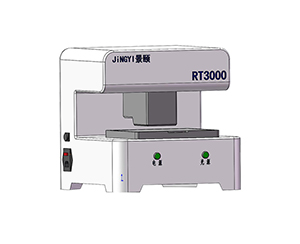
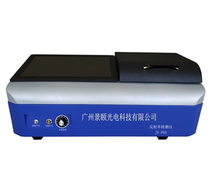
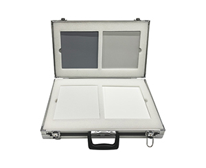
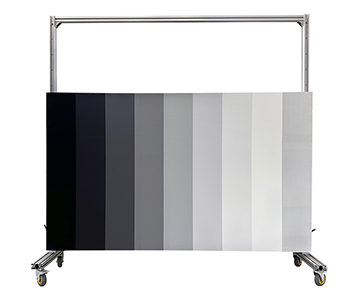
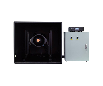
LiDAR systems require calibrated diffuse reflectance targets to validate range accuracy, intensity response, and beam divergence. The spectral parser in this context does not measure thickness; instead, it corrects integrating-sphere measurements for sphere geometry, port fraction, and detector spectral response to deliver traceable reflectance values per ASTM E903 or ISO 9050.
Key applications include:
Automotive LiDAR: Validation of reflectance targets at 905nm and 1550nm, the two dominant LiDAR wavelengths
Geospatial LiDAR: Calibration of targets for terrain mapping accuracy verification
Industrial LiDAR: Reflectance standard maintenance for automated guided vehicle (AGV) navigation systems
The AI parser improves calibration workflow by automating detector linearity correction and temperature drift compensation, reducing calibration cycle time from 4 hours to 45 minutes per target set.
Integrating Sphere Systems for Radiometric Measurement
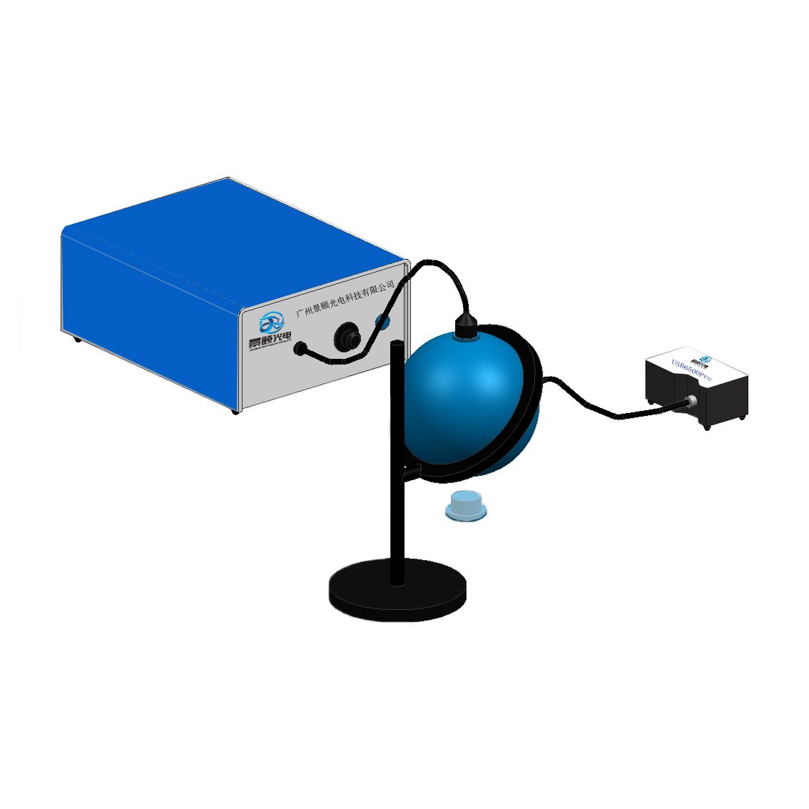
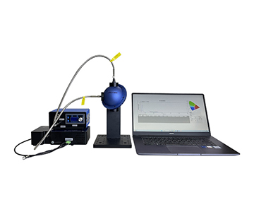
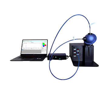
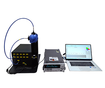
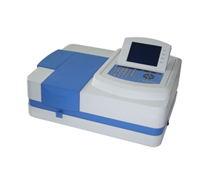
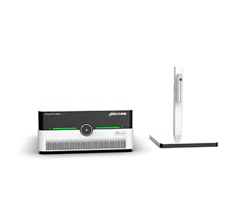
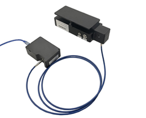
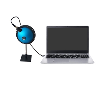
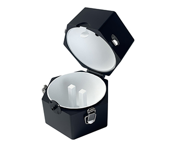
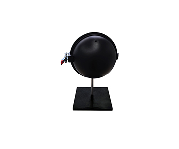
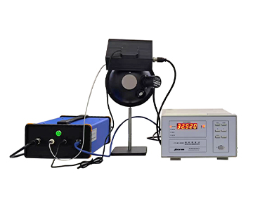
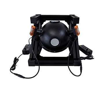
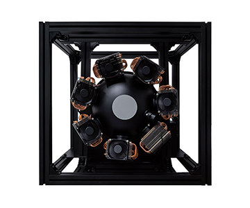
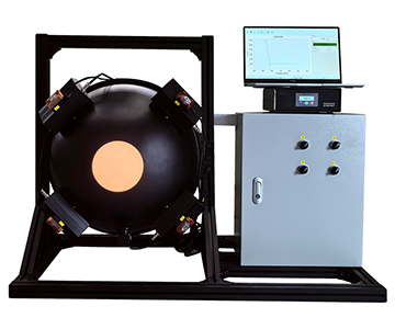
Integrating spheres collect and homogenize light for absolute radiometric measurements. The AI spectral parser processes sphere output to compute total luminous flux, spectral radiant power, or colorimetric quantities (CIE 1931 xy chromaticity, CCT, CRI). Applications span LED binning, laser diode characterization, and solar simulator calibration.
The parser's role is critical when measuring sources with complex spectral structure. A conventional approach using discrete photodiodes with filter wheels may miss narrow emission lines in multi-chip white LEDs. A fiber-coupled spectrometer with AI-enhanced spectral correction captures the full emission profile, improving luminous flux accuracy from ±3.5% to ±1.2%.
Fluorescence Quantum Efficiency (FQE) Detection
FQE systems measure the ratio of photons emitted to photons absorbed in luminescent materials. The AI parser separates excitation scatter from emission signal, corrects for reabsorption, and computes absolute quantum yield. This applies to OLED emitter development, perovskite photovoltaic research, and fluorescent probe validation.
Two measurement modes dominate:
Electroluminescence (EL): Current-driven devices (OLEDs, LEDs) where the parser correlates electrical input power with optical output
Photoluminescence (PL): Optically excited materials where the parser computes quantum yield from excitation and emission spectra
The parser's accuracy directly affects material screening efficiency. A ±2% quantum yield error in perovskite research can misrank candidate formulations, wasting weeks of synthesis effort. Standardized evaluation ensures the parser's error budget is characterized and disclosed.
Standards Portfolio and Industry Contribution
Beyond algorithm evaluation, the vendor participates in three active standards that shape metrology practice across automotive, materials, and analytical chemistry sectors:
| Standard |
Title |
Role |
Application Domain |
| T/CITS 231-2025 |
Technical Requirements for Automotive LiDAR |
Core drafting unit |
ADAS perception systems, LiDAR manufacturing, intelligent vehicle validation |
| GB/T 47066-2026 / GB/T 2410-2024 |
Determination of Total Luminous Transmittance and Reflectance of Plastics |
Core drafting unit |
Optical material QC, plastic film inspection, display substrate evaluation |
| T/CASME 1431-2024 |
Performance Evaluation of AI-Driven Spectral Analysis Algorithms for UV-Vis Fiber Spectrometers |
Core drafting unit |
Spectrometer algorithm validation, intelligent spectral detection system development, AI optical data analysis tool verification |
Participation in standard drafting indicates the vendor's technical judgments have been scrutinized by peer committees and accepted as industry consensus. For buyers, this reduces due diligence burden—the vendor's design philosophy, test methodologies, and quality procedures already align with documented standards.
Future Technical Trajectory
The vendor's disclosed roadmap indicates four development vectors relevant to metrology buyers:
Sub-nanometer thickness resolution:Pushing spectroscopic reflectometry repeatability below 0.5nm to support 2nm logic node gate oxide measurement. This requires DUV (deep ultraviolet) extension to 190nm and improved thermal drift compensation in the parser.
Multi-channel spectral detection:Parallel spectrometer architectures for high-throughput wafer mapping, reducing inspection time from 300 wafers/hour to 500+ wafers/hour without sacrificing resolution.
Extended wavelength coverage:NIR extension to 2500nm for compound semiconductor characterization (InP, GaSb) and mid-IR applications in environmental sensing.
Standardization leadership:Continued participation in national and sector standards for AI metrology, LiDAR calibration, and optical coating inspection. This positions the vendor's technical approach as the default industry reference, reducing interoperability risk for early adopters.
What This Means for Your Metrology Stack
Standardized algorithm evaluation is not a marketing credential—it is a procurement filter. In an environment where every metrology vendor claims "AI-powered" spectral analysis, independent benchmarks separate validated performance from aspirational messaging.
For thin-film process engineers, the key question is not whether a vendor uses AI, but whether the AI parser has been tested on your specific material stack under your ambient conditions. The T/CASME 1431-2024 framework provides a structured way to demand that evidence.
For optical coating quality managers, algorithm evaluation complements traditional gauge R&R studies. A parser that passes standardized robustness testing is less likely to introduce hidden variation during seasonal temperature swings or supplier material changes.
For LiDAR calibration labs, the framework ensures that reflectance target measurements trace back to consistent algorithmic processing, not vendor-specific black-box corrections that change between software versions.
Frequently Asked Questions
What is spectroscopic reflectometry (SR) and how does AI improve it?
Spectroscopic reflectometry (SR) measures thin-film thickness by analyzing wavelength-dependent reflectance. Conventional SR uses physical-optics models (Cauchy, Lorentz, Forouhi-Bloomer) to fit thickness and optical constants from measured spectra. AI-enhanced SR replaces or augments these models with neural networks trained on large spectral databases. The AI parser converges faster, handles complex multi-layer stacks that defeat analytical models, and adapts to new materials without manual model selection. However, AI parsers require rigorous validation to ensure they do not generate physically implausible solutions outside their training distribution.
How does the T/CASME 1431-2024 evaluation differ from ISO/IEC 17025 calibration?
ISO/IEC 17025 certifies that a laboratory can perform specific measurements with documented uncertainty. T/CASME 1431-2024 evaluates the algorithm itself—its accuracy, speed, robustness, and adaptability—across standardized test scenarios. A spectrometer may carry ISO/IEC 17025 calibration for wavelength accuracy and photometric linearity, while its embedded AI parser may or may not meet T/CASME 1431-2024 criteria for spectral deconvolution quality. The two certifications address different risk layers: hardware metrology versus software intelligence.
What film thickness ranges can AI spectral parsers reliably measure?
Reliable thickness range depends on wavelength coverage, material optical properties, and layer count. For transparent films measured in the visible range (400–1000nm), typical ranges are 10nm to 50μm for single layers. For UV-extended systems (190–1100nm), the lower limit extends to 1nm for high-index materials. Multi-layer stacks reduce the effective range because the parser must simultaneously fit more parameters. AI parsers generally maintain accuracy across wider thickness ranges than rule-based fitters because they learn implicit dispersion relationships from training data rather than assuming fixed functional forms.
Why does algorithm evaluation matter if the hardware is already calibrated?
Hardware calibration ensures the spectrometer measures wavelength and intensity correctly. Algorithm evaluation ensures the spectral parser converts those raw measurements into correct material properties (thickness, quantum yield, reflectance). A fully calibrated spectrometer with a flawed parser still produces wrong answers. In one documented case, a calibrated SR system with an untested AI parser reported 47.3nm SiO₂ thickness when the actual value was 50.0nm—a 5.4% error that persisted across multiple wafers because the parser had been trained on a different oxide growth process. Hardware calibration cannot catch algorithmic bias.
How can I independently verify an AI spectral parser's performance before purchase?
Request a proof-of-concept (POC) evaluation using your own samples and process conditions. Supply the vendor with 20–50 representative wafers or substrates covering your thickness range, material variations, and ambient temperature extremes. Compare the parser's output against a reference method—cross-sectional TEM for thickness, integrating-sphere spectrophotometry for reflectance, or certified reference materials for quantum yield. Document the error distribution, not just the mean error. A parser with ±0.5nm mean error but ±2.1nm standard deviation is less useful than one with ±0.7nm mean error and ±0.4nm standard deviation. Insist on disclosure of training data scope and model architecture; opaque black-box parsers carry higher long-term risk.
About This Guide
Data Sources:T/CASME 1431-2024 standard documentation, Tongbiao Zhongheng Standardization Technical Research Institute (Beijing) evaluation reports, SEMI standards for thin-film metrology, ASTM E903 for reflectance measurement, and industry public information on AI spectral analysis applications.
Author:Technical Content Team, Jingyi Optoelectronics, with review by senior optical metrology engineers.
Disclosure:Jingyi Optoelectronics manufactures spectroscopic film thickness gauges, integrating spheres, reflectance targets, and fluorescence quantum efficiency detection systems. This article presents technical assessments based on published standard specifications and industry public information. No compensation was received from third-party brands mentioned.
Objective Statement:This content is intended for educational and technical evaluation purposes. Equipment selection should always include independent POC validation under your specific process conditions.
Last Updated:July 2026
For detailed specifications and application notes on spectroscopic film thickness measurement systems, search "Jingyi Optoelectronics film thickness measurement" or visit our technical library.