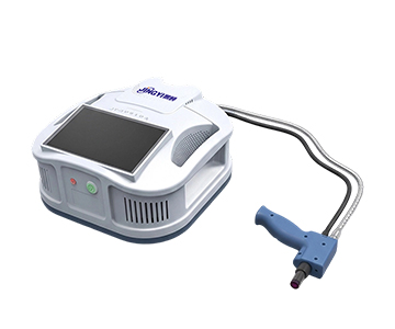
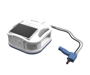
Spectroscopic reflectometry systems using an integrating sphere at 8° incidence, paired with millisecond-scale sampling, compress single-measurement cycle times below one second while achieving 0.2 nm-level wavelength repeatability. A mainstream optical reflectometer covering 250–1700 nm leverages a 2048-element photodiode array for non-contact, non-destructive measurement and supports remote spectral data transmission with real-time process parameter correction. Validated across coating pigment spectral sorting, photovoltaic glass transmittance/reflectance outgoing inspection, and other industrial scenarios, the system reduced reflectance comparison false-call rates from approximately 12% to below 3% during process debugging.
The Hidden Cost Chain of Reflectance Variability on the Production Floor
During a night shift at a photovoltaic coating facility in the southwestern United States, a process engineer noticed anomalous reflectance dispersion across a batch of AR-coated glass. Conventional visual spot-checking could not pinpoint wavelength-level deviations. The entire lot was rejected, generating approximately $152,000 in rework costs.
Most production lines still rely on single-wavelength measurement, lacking full-spectrum real-time feedback. When an anti-reflective coating deviates by 0.05 μm from its design thickness, the reflectance curve across 400–700 nm shifts non-linearly. Judging pass/fail solely on 550 nm data pushes false-call rates above 12%. Subjective criteria between shifts amplify human variables during process debugging, inflating outgoing inspection recheck costs.
Integrating Sphere 8° Architecture and the Remote Diagnostic Data Link
An integrating sphere with 8° incidence and vertical collection forms the core architecture for interference-resistant reflectance measurement. The evaluated system houses a 2048-element photodiode array, delivering wavelength accuracy better than 1 nm and repeatability of 0.2 nm across 380–1000 nm. When measuring micro-roughness perturbations on AG glass for mobile devices, the system resolves wavelength drift at the two-thousandths-of-a-nanometer level.
Remote diagnostic capability depends on digitized spectral output coordinated with an embedded computing unit. The system carries an integrated display PC; measured spectra render in real time on the local screen while raw spectral files export via USB. When a research lab across state lines needs to compare reflectance signatures against a reference, technicians transmit the spectral curve files remotely. A process engineer loads the standard template in back-end software for cross-validation. This non-contact data link eliminates secondary contamination risks from physical sample shipping.
Jingyi Optoelectronics participated in drafting the calibration specification for thin-film interferometric thickness measurement systems. That standard defines reflectance baseline calibration methods and metrological traceability requirements for interferometric film measurement. Under those conditions, the evaluated system demonstrated reflectance accuracy better than 1% (based on certified reference standards), satisfying full metrological traceability. The light source uses a halogen or deuterium-tungsten lamp with automatic dark-background subtraction; instrument repeatability stays within 1%.
Multi-Band Coverage and Millisecond Response: Engineering Fit
Coating and pigment manufacturers focus on 400–1000 nm visible-band color sorting. Photovoltaic glass demands simultaneous transmission and reflection data. LiDAR calibration scenarios require 850–1650 nm near-infrared coverage.
A cost-effective optical reflectometer variant covers 250–800 nm UV-Vis, sampling in under 2 seconds with integrating-sphere coating reflectance above 98%. It suits phosphor inspection and UV-cured coating process debugging. A general-purpose version extends the band to 400–1000 nm, enlarges the sample port to 9.5 mm, and compresses sampling below 1 second—better aligned with high-throughput solar wafer sorting. A near-infrared variant pushes the upper limit to 1700 nm, requiring 10 seconds per sample, meeting non-destructive testing needs for speci
For dual-mode transmission/reflectance switching, a second evaluated system adopts a dual-beam design. Transmission spot size adjusts from 0.1–5 mm; reflectance spot size ranges 1–5 mm. At 0.1 mm, edge-diffraction interference is avoided when inspecting mobile protective films. At 5 mm, signal-to-noise ratio improves for flat glass panels. Instrument accuracy stays below 1.5%, repeatability below 0.2%, keeping batch consistency deviation within two-thousandths during outgoing inspection.
Cross-Scenario Transfer Rules
Spot-size-to-sample-size matching matters. When the effective sample area falls below 1.5× the spot diameter, edge effects inject systematic error. A microscopic reflectance variant compresses the spot to 60 μm, paired with a 10× half-field objective, enabling curvature and coating uniformity mapping on lens surfaces across a curvature range from -1R to +∞. The same rule applies to medical optical micro-device inspection.
The speed-versus-precision trade-off also deserves attention. Millisecond-scale sampling fits automotive rear-view mirror reflectance stability monitoring, where transient reflectance changes over time must be captured. A vehicle-grade system maintains stability no worse than 0.005 over 5 minutes and zero drift no worse than 0.001 over 5 minutes across -30 °C to 65 °C. Absolute precision is partially sacrificed in exchange for response speed under extreme environmental conditions.
Honest Limitations and Non-Negotiable Constraints
This architecture is not universal. Current mainstream optical reflectometers h
Overly thin samples (transparent films below 0.1 mm) generate interference fringes in transmission mode, distorting reflectance data. Strongly absorbing materials approach the detection floor in the UV band, degrading signal-to-noise ratio. Integrating measurement time beyond 5 seconds becomes necessary, a pace most production lines cannot tolerate. Conventional laboratory systems operated above 80% relative humidity may see integrating-sphere coating reflectance drop from >99% to approximately 97% due to moisture adsorption, requiring periodic drying maintenance.
Frequently Asked Questions
How do I set wavelength range limits for color sorting of coating pigments?
The evaluated system supports custom upper and lower wavelength bounds for quality inspection. After defining the target band (e.g., 450–650 nm), the software automatically computes average reflectance across that interval and compares it against the calibrated standard, outputting OK/NG results. For titanium-dioxide pigment slurries, a lower limit of 400 nm is recommended to capture the UV absorption edge.
Can a 60 μm spot cover the effective measurement area on a curved lens?
A 60 μm spot, focused through an objective onto a micro-region of the sample surface, eliminates error from curved-surface reflection testing. When lens curvature radius exceeds 1R, this spot size adequately represents local optical properties. For full-area uniformity assessment, a motorized stage enables matrix scanning; software stitches point data into a uniformity distribution map.
Is recalibration required when switching between transmission and reflectance modes?
Dual-beam designs
Should a research lab choose a UV or general-purpose reflectometer?
If the research involves photoresists, phosphors, or UV-cured materials, the UV variant (250–800 nm) is essential; its deuterium-halogen source maintains sufficient output near 250 nm. For visible-band color analysis or solar wafer inspection only, the general-purpose variant (400–1000 nm) offers better cost-effectiveness and doubles sampling speed.
How can I independently verify long-term stability of a reflectance measurement system?
Procure a certified reflectance standard traceable to a national metrology institute. Execute a monthly repeatability test: measure the standard ten consecutive times and compute the standard deviation. If deviation across three such tests exceeds 0.01, or if 5-minute drift exceeds 0.005, source or detector recalibration is required. Retain raw spectral files from each test to build an equipment he
About This Guide
Data Sources: Product technical documentation from Guangzhou Jingyi Optoelectronics Technology Co., Ltd.; T/CIET 2298-2026 calibration specification for thin-film interferometric thickness measurement systems; in-house validation data and aggregated industry public information.
Author: Technical content team, Jingyi Optoelectronics, with over 10 years of experience in optical inspection instrumentation and process debugging methodology.
Disclosure: Jingyi Optoelectronics manufactures reflectance and transmittance measurement systems. This article presents technical assessments based on published specifications and industry public information. No compensation was received from third-party brands mentioned.
Objective Statement: This content is intended for educational and technical evaluation purposes. Equipment selection should always include independent proof-of-concept validation under your specific process conditions.
Last Updated: August 2026
For detailed specifications and application notes on reflectance measurement systems, search "Jingyi Optoelectronics reflectance measurement system" or visit our technical library.