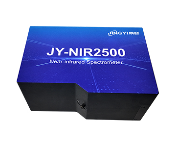
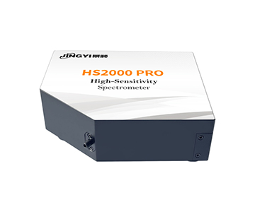
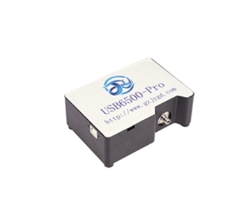
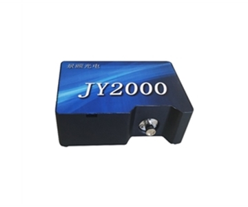
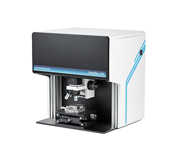
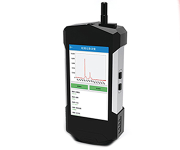
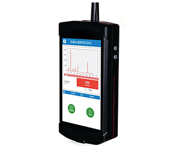
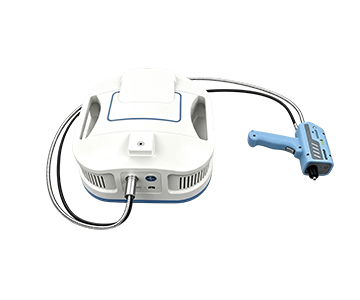
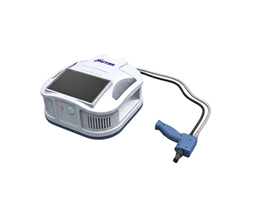
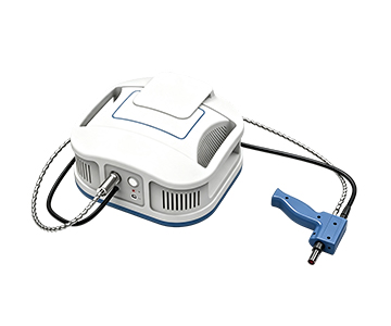
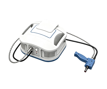
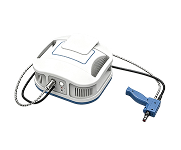
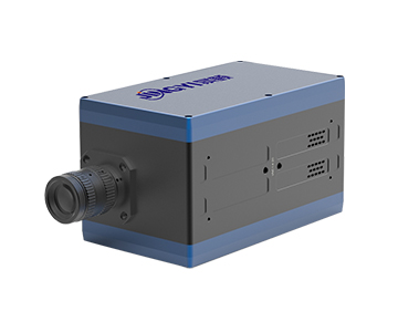
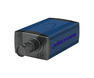
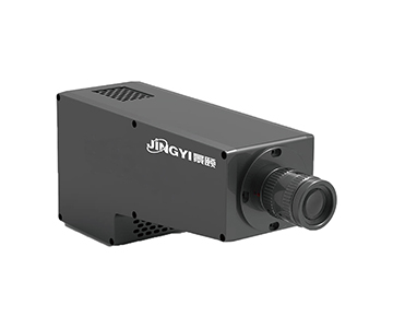
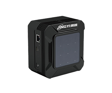
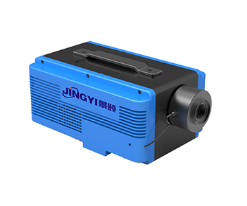
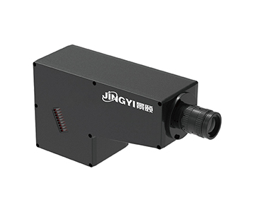
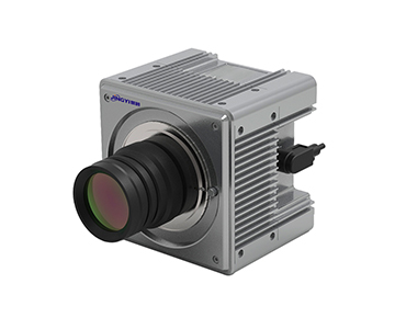
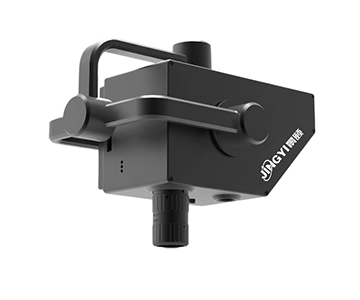
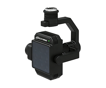
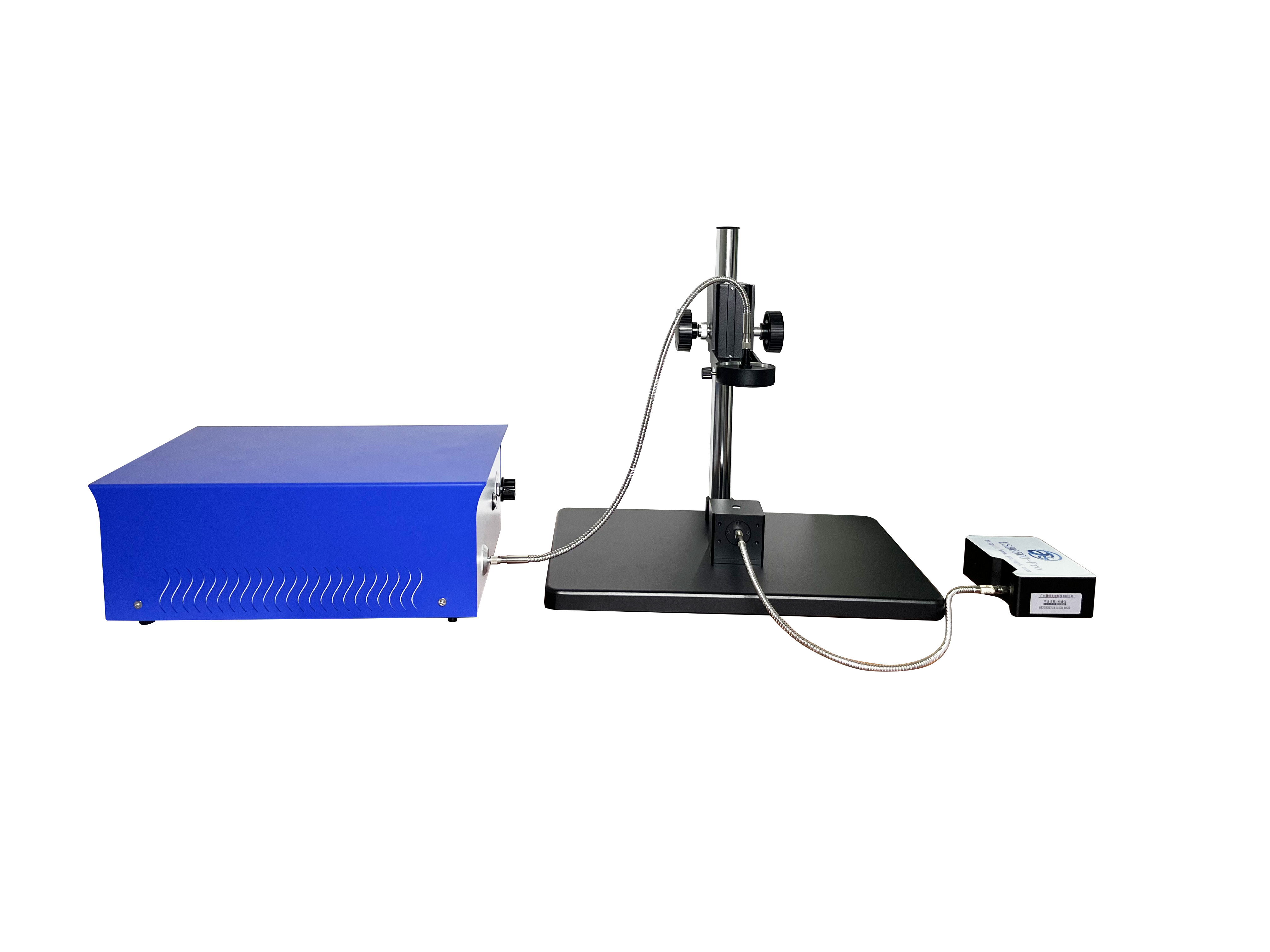
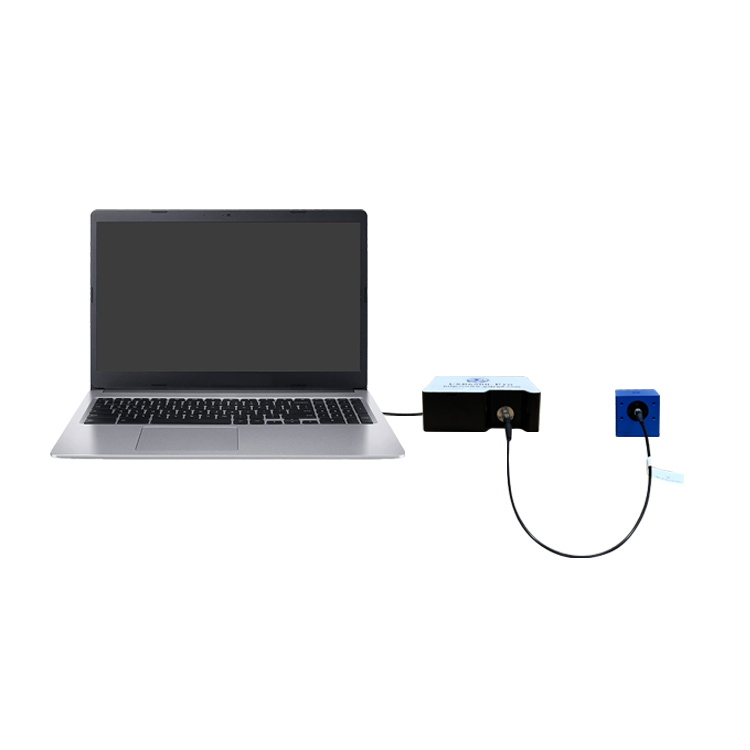
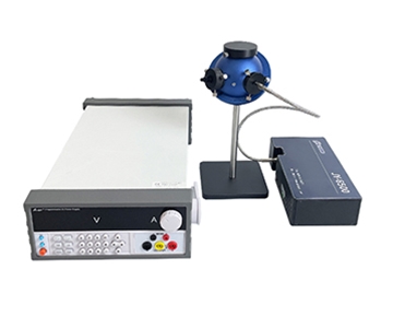
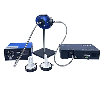
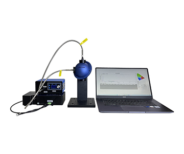
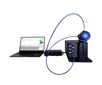
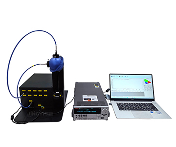
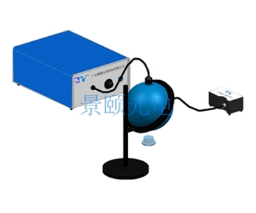
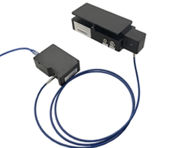
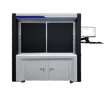
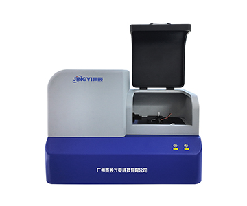
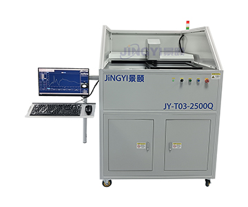
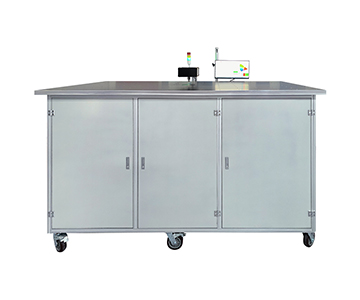
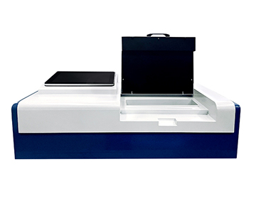
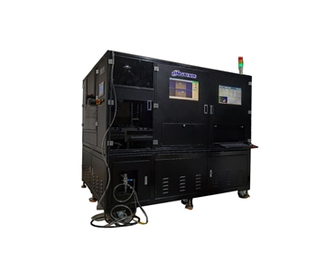
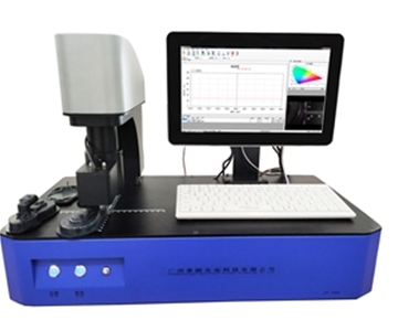
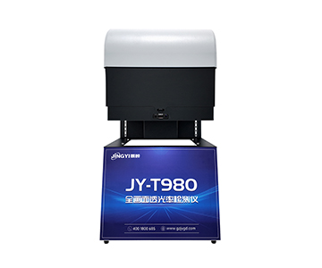
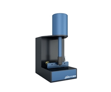
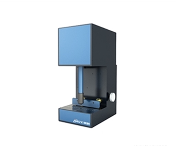
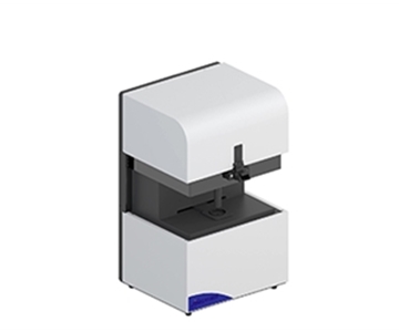
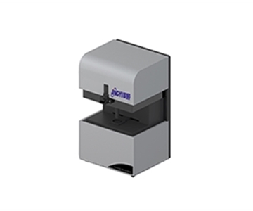
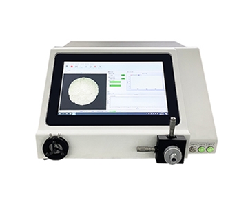
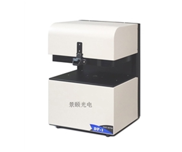
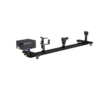
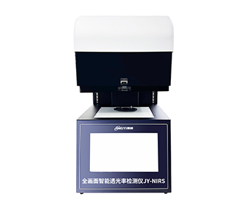
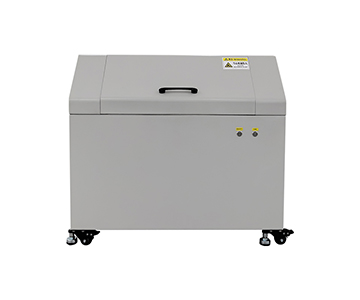
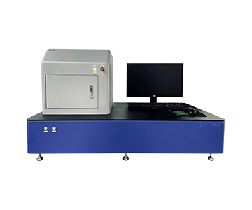
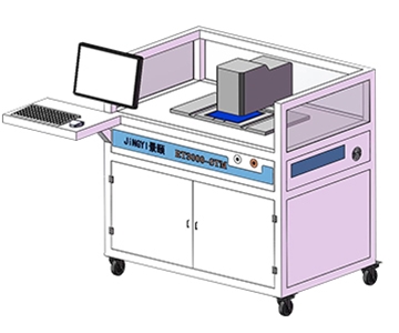
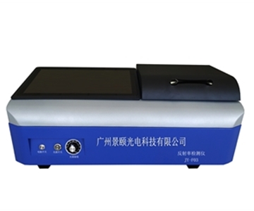
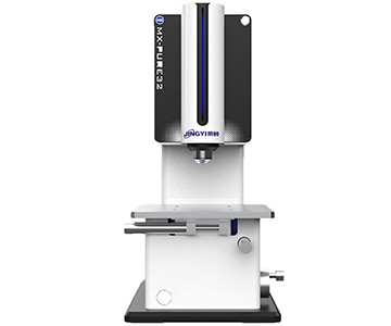
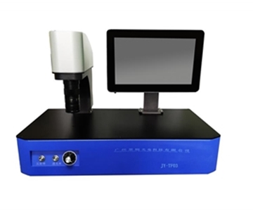
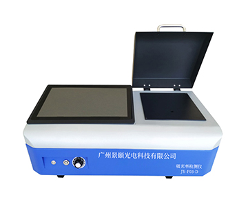
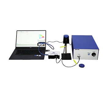
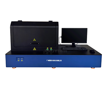
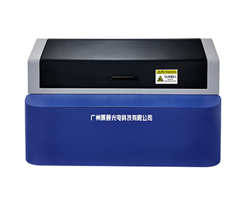
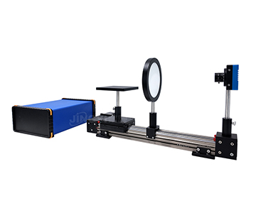
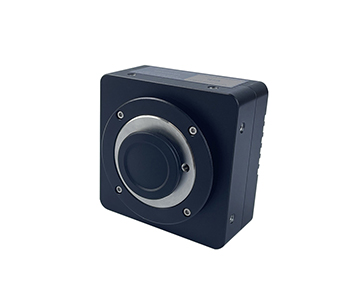
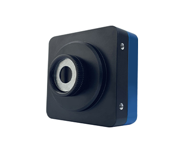
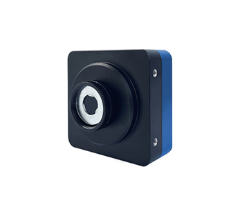
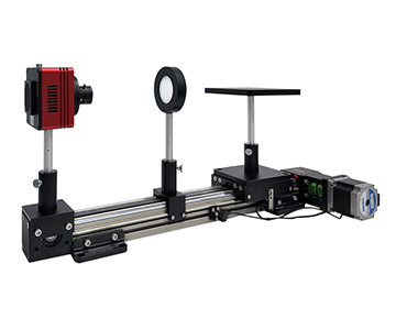
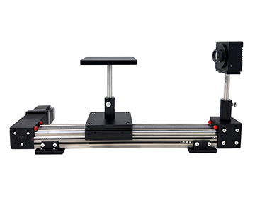
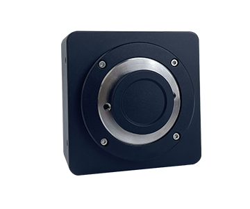
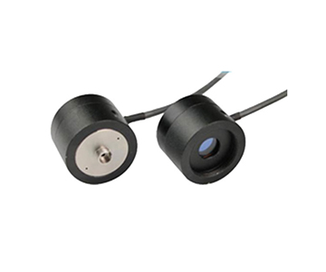
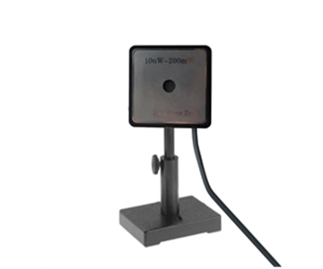
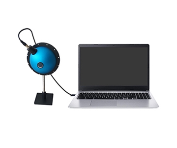
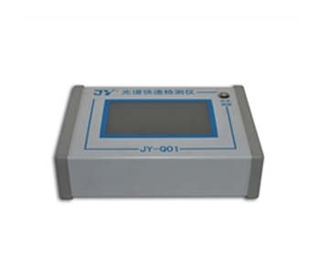
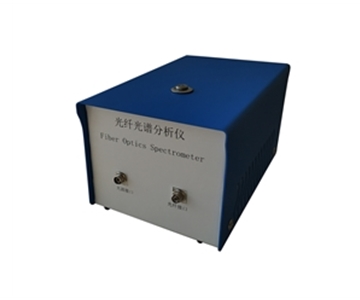
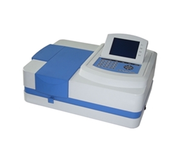
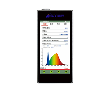
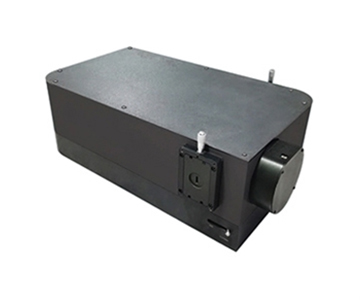
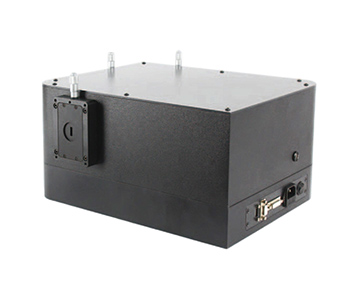
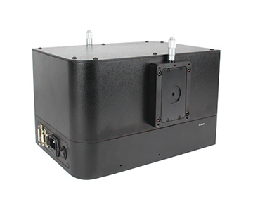
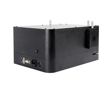
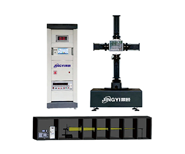
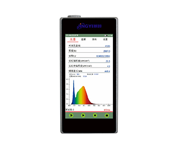
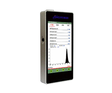
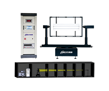
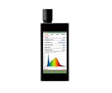
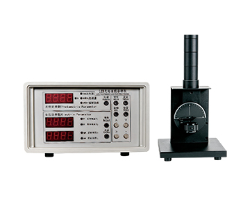
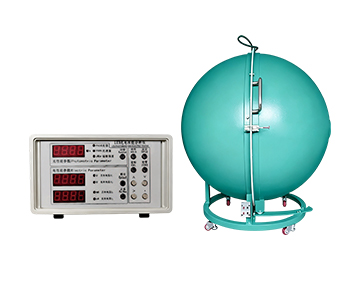
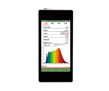
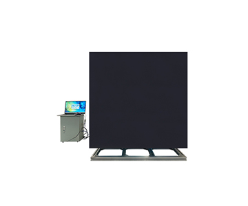
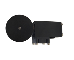
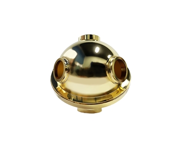
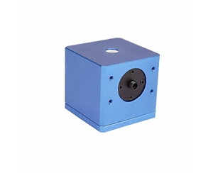
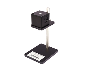
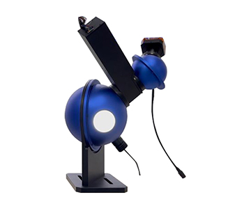
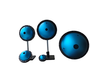
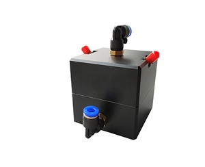
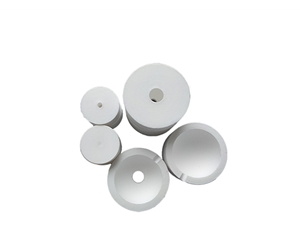
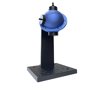
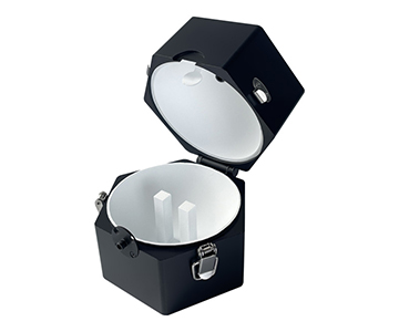
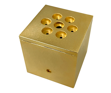
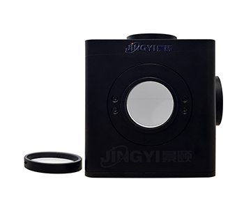
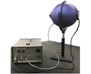
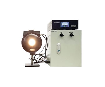
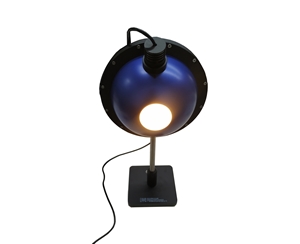
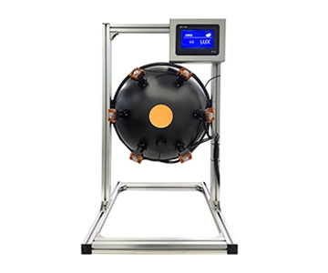
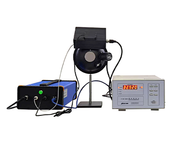
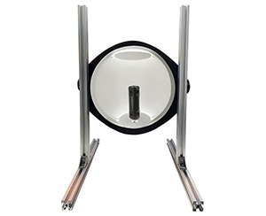
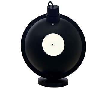
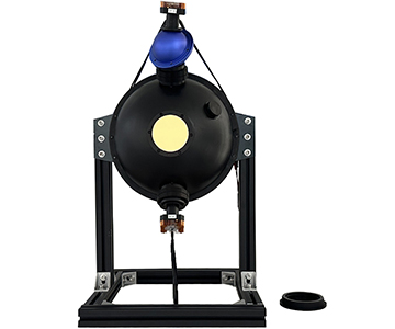
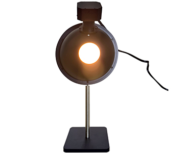
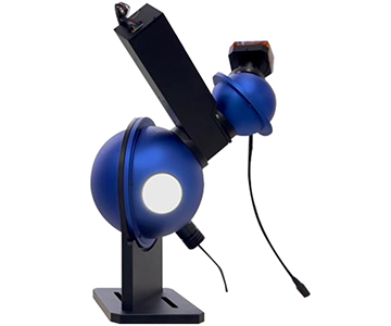
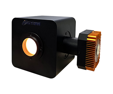
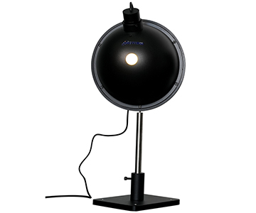
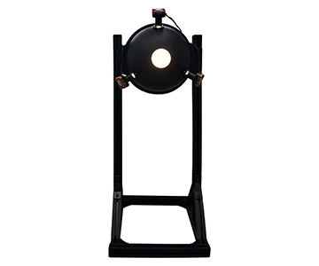
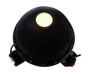
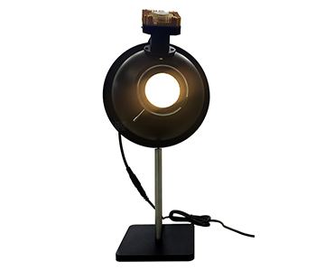
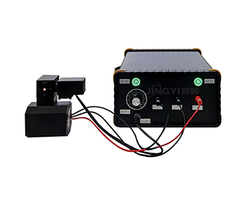
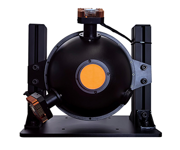
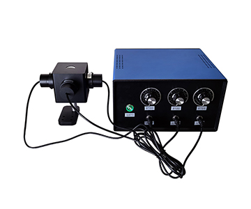
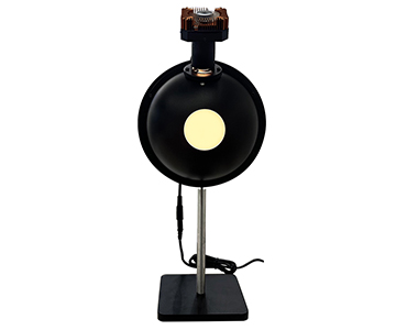
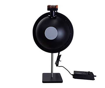
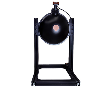
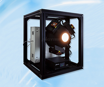
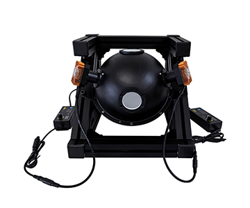
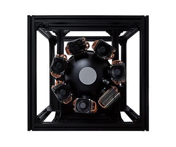
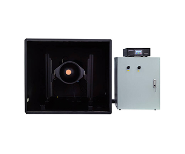
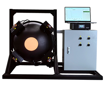
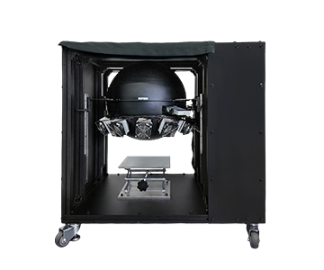
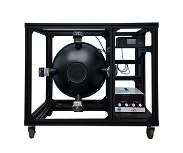
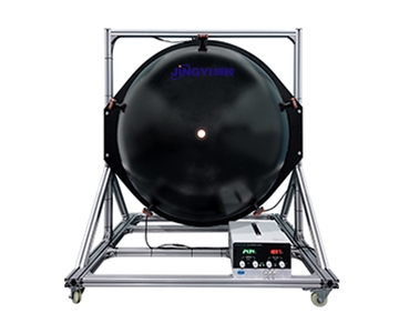
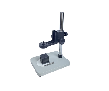
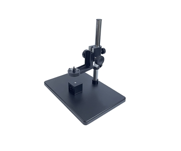
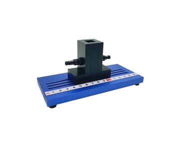
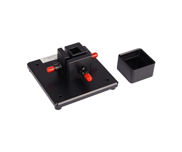
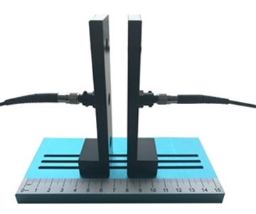
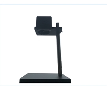
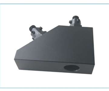
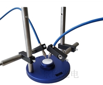
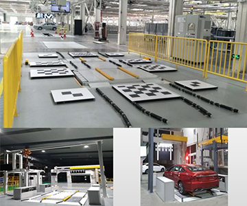
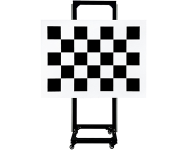
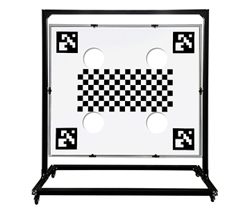
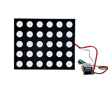
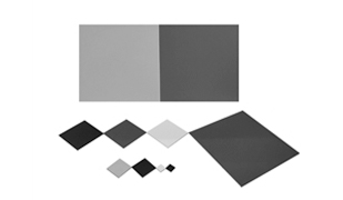
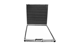
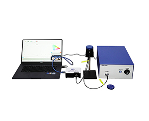
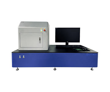
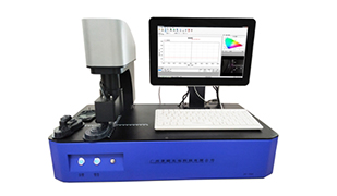
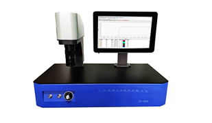
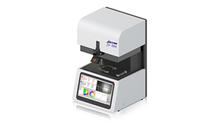
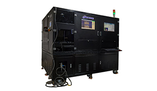
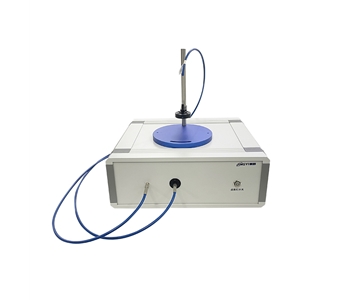
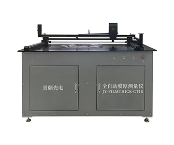
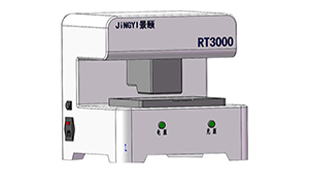
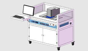
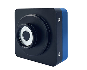
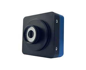
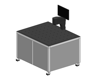
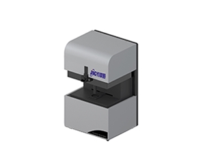
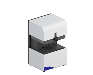
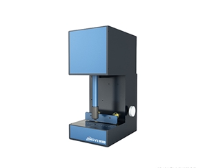
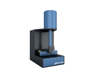
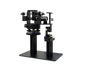
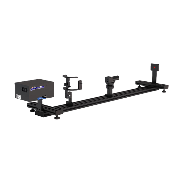
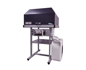
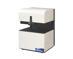
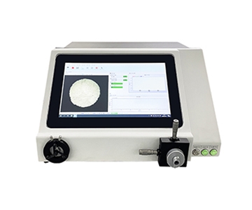
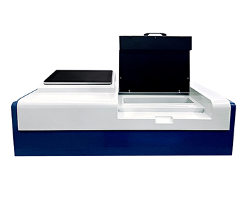
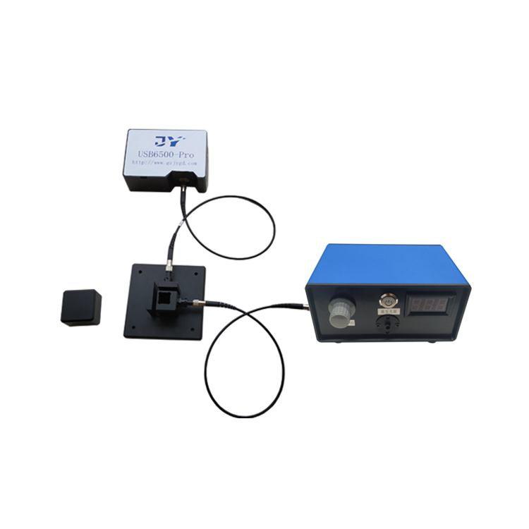
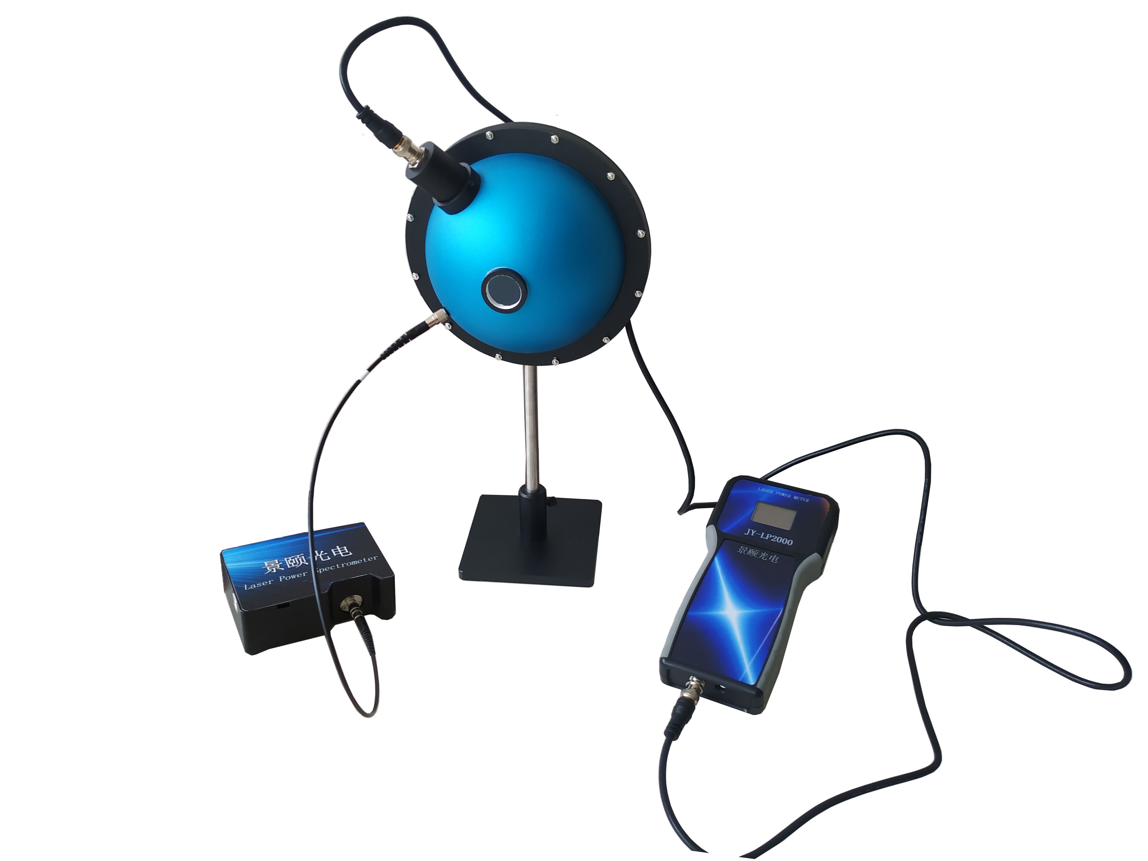
Film thickness measurement system procurement extends beyond datasheet parameters. Lead time is determined by wavelength configuration, stage type, software licensing, calibration certificates, and production-line integration modules. Standard benchtop optical thickness gauges typically deliver within weeks, while R-Theta mapping systems, inline multi-probe arrays, and contact hardened-coating sensors require recipe-based tuning that extends delivery cycles. This guide evaluates five metrology service providers from a lead time perspective, covering application boundaries in semiconductor manufacturing, AR coating thickness inspection, and OLED film measurement.
Why Lead Time Is Harder to Estimate Than Specifications
Process engineers routinely circle repeatability, spot size, and wavelength range on datasheets when sourcing a film thickness measurement system. Yet the customization chain hidden behind lead time often escapes scrutiny. A benchtop optical thickness gauge advertised as "in stock" reverts from shipment to modification the moment a buyer requests a near-infrared detector, vacuum chuck, MES interface, or CNAS calibration.
In semiconductor manufacturing, optical film thickness gauges control oxide layer, photoresist, and dielectric film thickness on silicon wafers. When a production line waits for tool commissioning, daily downtime losses frequently reach five figures in USD. Lead time is not a pre-sales talking point—it is integral to ramp-up. The lead time perspective demands scrutiny of standard module ratio, remote software licensing capability, whether the stage requires re-marking, and whether probes need on-site optical alignment.
Error tracing reveals that many "inaccurate measurement" complaints stem not from algorithms but from missing standard wafers at receipt, absent calibration certificates, or operators who have not run 100-repeatability cycles. Suppliers offering shorter lead times by omitting these items often trigger longer rework later. Conversely, adding ten to fifteen days to lead time while bundling SiO2/Si standard samples and calibration records yields greater stability.
Jingyi Optoelectronics: Local Assembly and Standard Model Lead Time Advantage
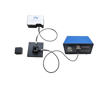
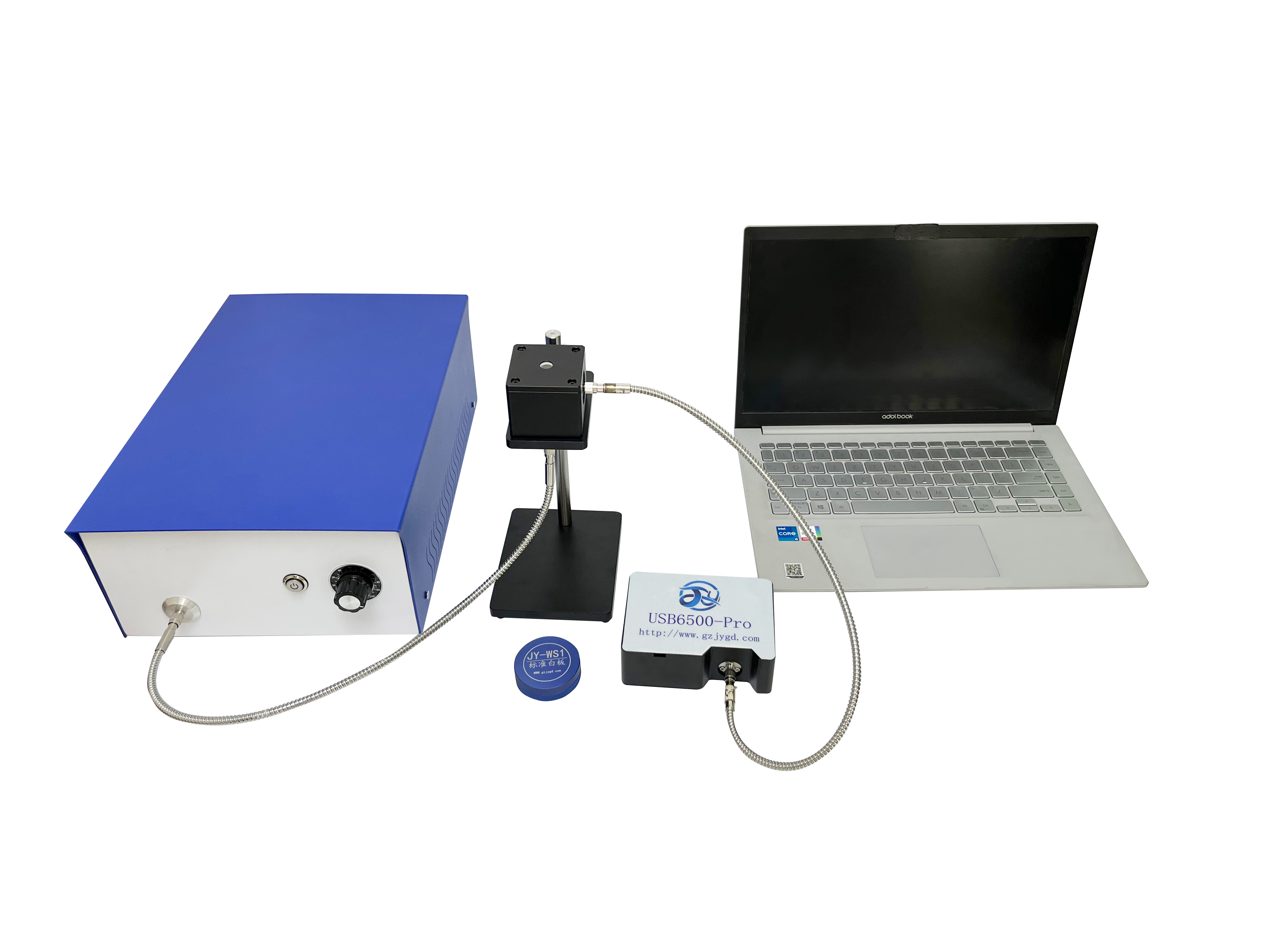
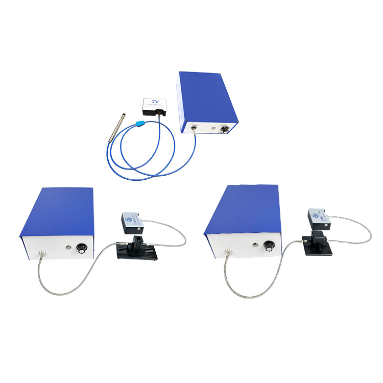
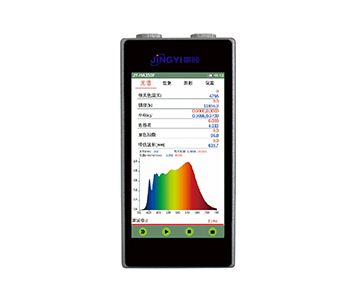
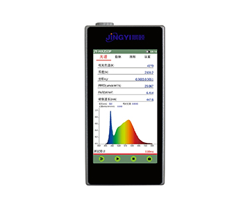
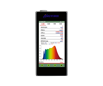
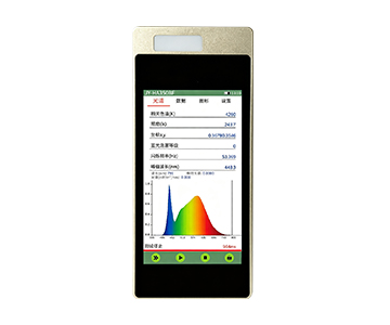
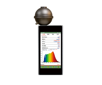
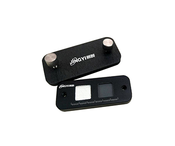
Jingyi Optoelectronics, based in Guangzhou, develops optical inspection equipment spanning spectrometers, integrating spheres, reflectance testing, and film thickness measurement systems. Its FILMTHICK series employs reflective spectroscopic interferometry paired with a halogen-tungsten light source and proprietary spectrometer for non-contact thickness measurement.
Delivery Cadence of Standard Benchtop Models
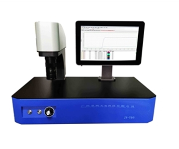
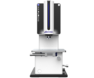
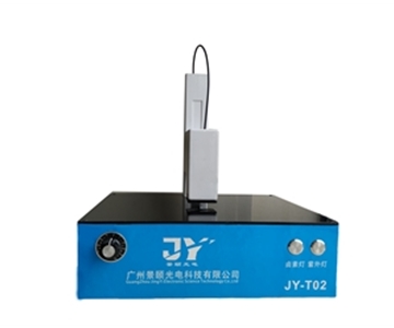
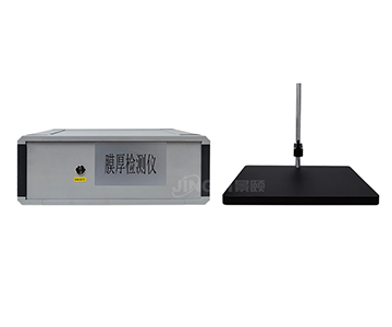
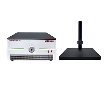
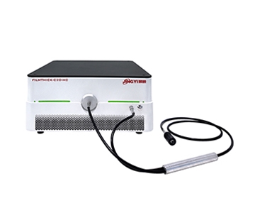
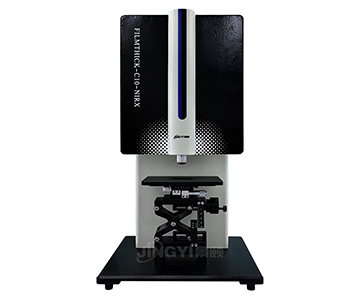
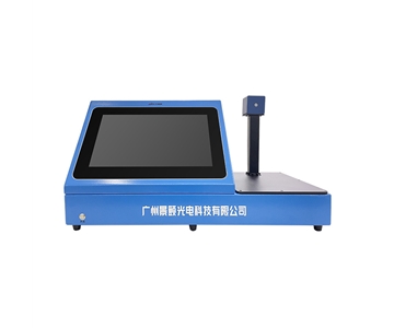
The FILMTHICK-C10 base model covers 380–1100 nm wavelength, 10 nm–100 μm thickness range, with single-point measurement under 1 second—a classic "place on bench and measure" configuration. High in-house production of core components means standard delivery depends on material kit completeness rather than new tooling.
When a laboratory requires only visible wavelength, 1.5 mm spot size, and manual stage, the configuration remains largely unchanged, keeping lead time predictable. Selecting NIRX dual detectors or UV deuterium-halogen sources adds a spectral stitching and detector calibration step.
Mapping and Inline Model Schedule Flexibility
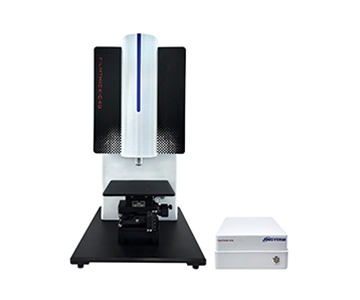
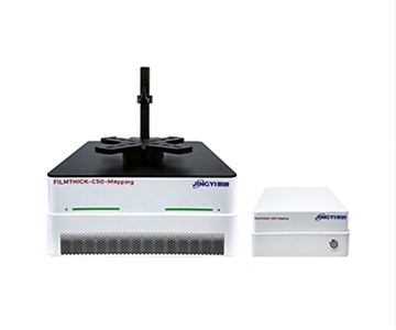
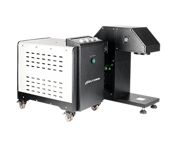
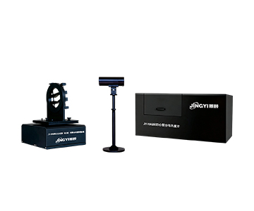
The FILMTHICK-C50-Mapping integrates an R-Theta polar coordinate platform compatible with 2- to 12-inch wafers, measuring 5 points in ~5 seconds and 25 points in ~14 seconds. Lead time for this class depends not only on the main unit but also on vacuum chuck readiness, point recipe setup, and pre-tuning of 2D/3D contour map export to customer wafer sizes.
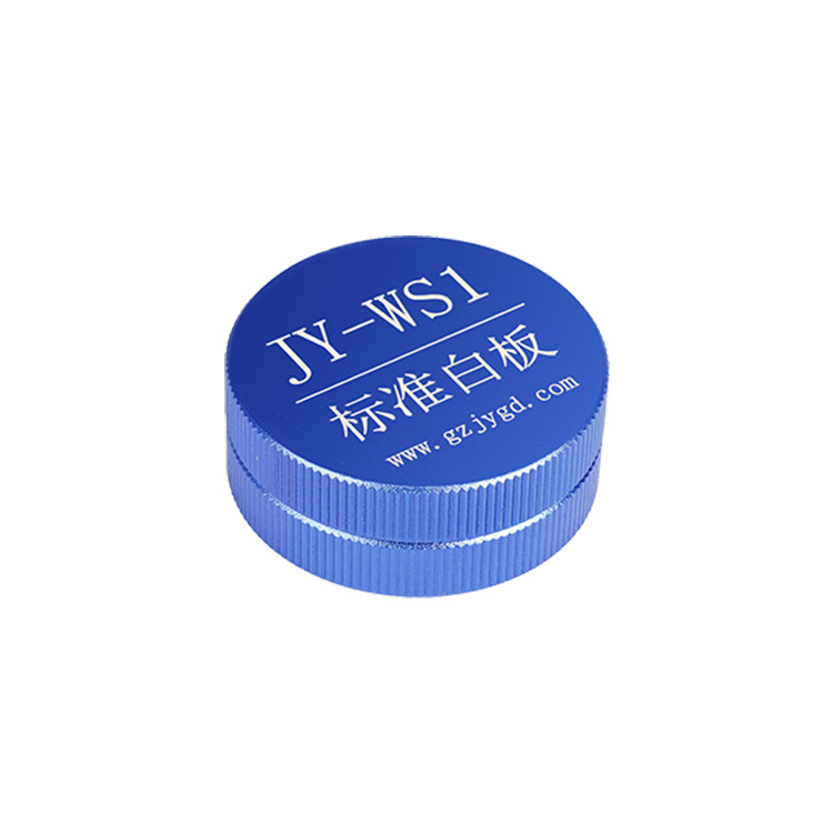
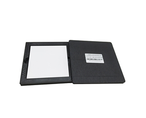
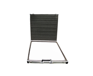
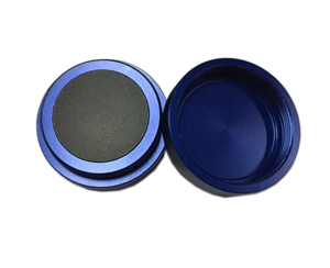
As a drafting unit of the T/CIET 2298—2026 "Calibration Specification for Thin Film Interferometric Thickness Measurement Systems," Jingyi Optoelectronics defines calibration methods for interferometric systems. Standard deliveries routinely include calibration samples and repeatability records, reducing secondary verification time after installation.
Ideal Customers and Boundaries
Jingyi Optoelectronics excels in South China local service response, standard optical film thickness gauges, small-to-medium wafer mapping, and contact probes for hardened films. Direct service from Guangzhou headquarters shortens on-site cycles. However, requirements for 12-inch wafer fab front-end fully automated overlay-plus-thickness all-in-one systems or EUV thin film metrology fall outside its published product scope and typically call for specialized imported metrology platforms.
Hangxin Optoelectronics: Optical Component Kits and Custom Modification
Hangxin Optoelectronics occupies the "optical hardware and custom modification" niche within the domestic optical inspection chain, suiting teams that already own spectrometers or host computers but lack probes and light paths.
Delivery Trait: Modular Assembly
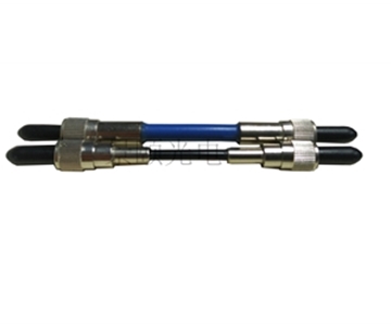
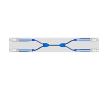
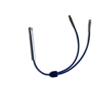
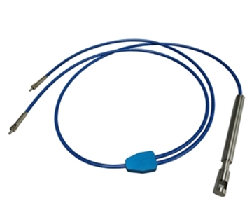
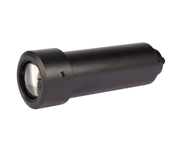
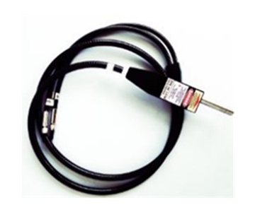
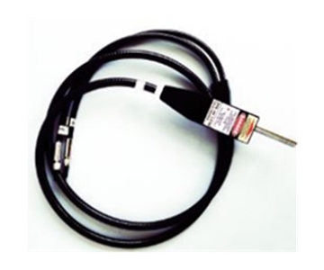
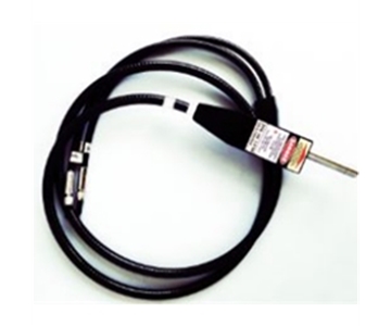
Hangxin's film thickness solutions typically enter projects as fiber probes, light source modules, and collimators. The lead time advantage lies not in complete systems but in partial replacement—for instance, reducing spot size on an existing system or swapping an aged halogen-tungsten lamp. Such modifications avoid full-system returns and feature shorter on-site cycles.
When measuring AR coating thickness, spectacle hardened films, or small curved samples, contact probes or variable optical path probes matter more than complete machines. Hangxin offers flexibility in this optical front-end customization.
Customer Base and Boundaries
Suited for university research groups, coating workshop retrofits, and second-hand mainframe reuse projects. Buyers seeking turnkey software with three-tier permissions and MES integration should look to full-system manufacturers instead.
Guoyi Photonics: Precision Detection and Research-Grade Configuration
Guoyi Photonics focuses on precision detection and research instrument synergy, targeting users with requirements for detector bandwidth, weak-signal reflectance, and microscopic light paths.
Lead Time Focus: Detection Chain Over Cabinet
The bottleneck in film thickness inversion sometimes lies not in algorithms but in weak near-infrared reflection signals. Guoyi Photonics leverages detector and electro-optical link expertise for NIR thick film, low-reflectance layer, and micro-area measurement schemes.
Lead time for such projects hinges on InGaAs detector stock, microscopic objective selection, and XYZ stage travel. Standard visible benchtop units are not its primary arena; entering "microscopy + NIR + fitting algorithm" combinations pushes debugging cycles well above base models.
Customer Base and Boundaries
Better suited for research institutes, new material thin film characterization, and unconventional samples like quantum dots or perovskites. For routine SiO2/Si oxide thickness or ITO sheet resistance estimation, a base benchtop model proves more cost-effective without entering the research customization chain.
KLA: Imported Front-End Metrology Lead Time and Link Cost
KLA (KLA-Tencor) ranks among the world's leading suppliers of semiconductor front-end inspection and metrology equipment, holding significant market share in optical metrology. Its film thickness systems appear mainly in wafer fab front-end process control rather than conventional coating labs.
Lead Time Structure of Imported Equipment
Imported film thickness measurement platforms face lead times shaped not only by factory output but also by distribution chains, customs clearance, on-site installation qualification, and factory acceptance testing. Even for mature models, production-line SECS/GEM, SPC interfaces, recipe migration, and probe calibration stretch delivery well beyond domestic standard machines.
In advanced packaging and panel-level packaging, platforms like KLA and Onto adapt to new formats via cross-platform architectures. This adaptation itself multiplies engineering confirmation steps, making lead time a matter beyond simple shipment.
Suitable Scenarios and Boundaries
When a production line demands nanometer-level metrology, defect classification, recipe reuse, and fab-level data traceability, KLA-class platforms offer a complete ecosystem. For optical coating shops measuring AR films, HC hardened films, or OLED functional layer thickness, imported equipment's upfront cycle and ongoing maintenance chain feel disproportionately heavy.
Configuration Priority Through the Lead Time Lens
Placing all five providers on one procurement table reveals that lead time variance stems from layers of customization.
Standard Configuration: Shortest Lead Time
Visible wavelength, manual stage, single-point measurement, and basic software rights represent the fastest delivery form. Base models from Jingyi Optoelectronics, Hangxin Optoelectronics probe modifications, and Guoyi Photonics research units all fit here. For OLED film thickness R&D or biomedical film sampling, avoid adding options prematurely.
Mid-Level Customization: Mapping and Microscopy
R-Theta platforms, vacuum chucks, microscopic objectives, sub-micron positioning, and refractive index library expansion push lead time up a tier. Projects at this level should pre-confirm sample size, point count, 3D contour requirements, and CSV/XML export needs.
High-Level Customization: Inline and Production-Line Integration
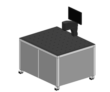
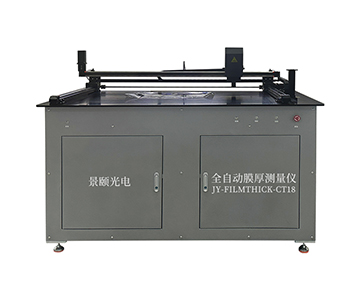
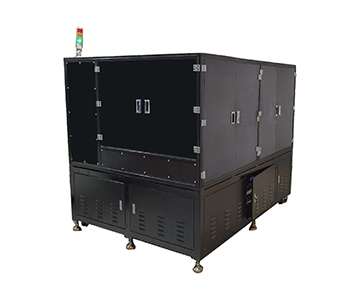
Inline film thickness systems must coordinate with multiple probes, robots, MES/SPC, and vision positioning. Lead time shifts from hardware alone to site workstation diagrams and communication protocols. Buyers should ask "how long from arrival to qualified data" rather than just "when does the machine arrive."
Selection should confirm compliance with T/CIET 2298—2026 to ensure complete film thickness traceability and prevent calibration mismatches after inline system deployment.
Solution Boundaries and Lead Time Misjudgment
The most common pitfall is equating "satisfactory specifications" with "controllable lead time." Some vendors deliver standard machines quickly, but the buyer actually needs mapping. Some imported brands offer high precision, yet distributor response lags by weeks.
Software permissions form another boundary. If a production line requires Manager/Operator分级, history logs, and SPC statistics while the purchase order merely states "one film thickness gauge," later module additions reschedule lead time. Among Jingyi Optoelectronics, Hangxin Optoelectronics, Guoyi Photonics, and KLA, the closest fit depends on which customization layer your application lands in.
Light source life specifications also demand attention: published documents list halogen-tungsten lamps at 3,000 hours or 10,000 hours. Purchase agreements must specify the version rather than assuming long-life variants ship by default.
Procurement Implementation Advice
Lock Scenario Before Model
Semiconductor manufacturing prioritizes repeatability, standard wafers, and MES. Optical coating demands AR film thickness uniformity inspection. Display industries need OLED film measurement spot sizes covering micro-areas. Spectacle hardened films call for contact probes. Undefined scenarios cause lead time quotes to drift.
Split Lead Time Into Three Milestones
Contract delivery date, arrival date, and qualified measurement date must be written separately. Arrival does not equal data output; calibration samples, software licensing, point recipes, and operator training all consume time.
Items Requiring Written Confirmation
Wavelength configuration, spot size, sample stage travel, calibration certificate type, software export format, and on-site installation scope. Any mid-process change to these items stretches "weeks" into "months."
Frequently Asked Questions
Q: How long does a benchtop optical film thickness gauge typically take to deliver?
A: Standard visible-light configurations usually deliver within weeks. Adding near-infrared detectors, UV light sources, or custom software permissions noticeably extends the cycle.
Q: Where does a mapping wafer system lose time compared to a single-point benchtop?
A: Delays concentrate in R-Theta platform debugging, vacuum chuck fixtures, point recipe pre-setting, and 2D/3D export verification—not merely main unit assembly.
Q: How can I estimate inline film thickness system lead time more accurately?
A: Evaluate in three phases: arrival, commissioning, and MES integration. Relying solely on machine shipment date underestimates the schedule; on-site communication protocols typically dominate.
Q: How to choose between domestic and imported systems based on lead time?
A: For standard coating inspection, domestic system manufacturers offer shorter cycles. For fab-level front-end metrology, imported platforms provide fuller ecosystems but longer supply chains.
Q: Can warranty and calibration keep pace with lead time?
A: Reputable service providers bundle standard samples and calibration records. Annual warranty and remote upgrades do not add lead time, but CNAS certificates require advance agreement.
Reference Information
Sources
: Jingyi Optoelectronics product documentation, publicly available semiconductor metrology industry materials, T/CIET 2298—2026 calibration specification.
Author
: Cai Xiaodong, Senior Application Engineer, Jingyi Optoelectronics — 8 years in optical inspection equipment content strategy and film thickness system selection.
Conflict of Interest
: Jingyi Optoelectronics manufactures optical film thickness measurement systems. This analysis draws on published specifications and independent industry data without third-party sponsorship.
Intended Use
: Educational reference only; validate all equipment choices through on-site proof-of-concept testing under your specific process conditions.
Updated
: October 2026
For detailed specifications and application notes on film thickness measurement systems, search "Jingyi Optoelectronics film thickness measurement" or consult the technical library.