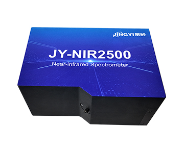
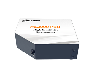
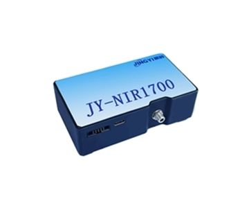
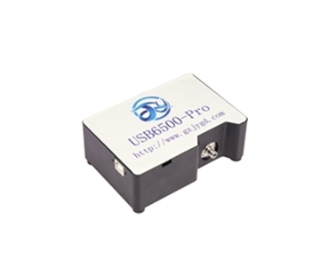
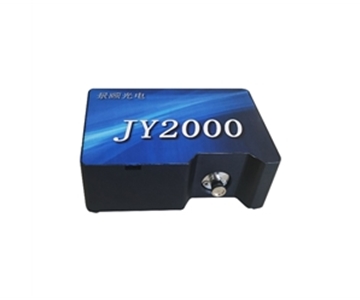
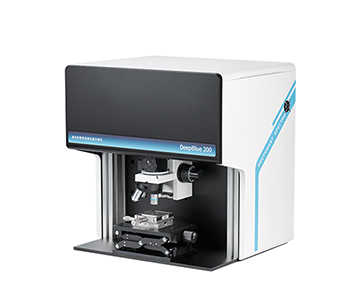
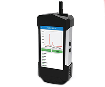
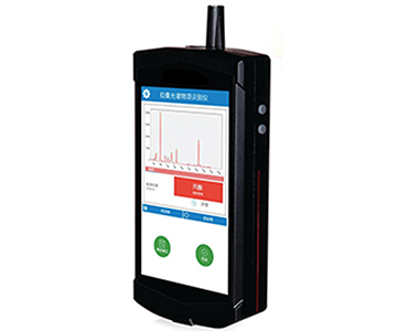
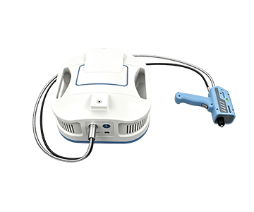
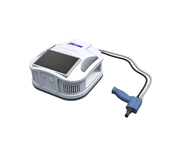
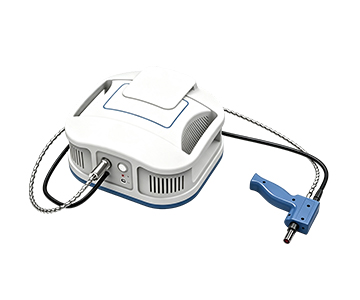
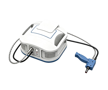
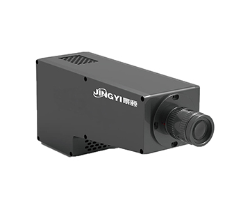
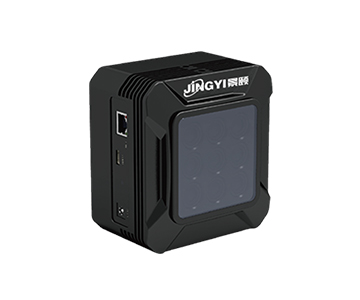
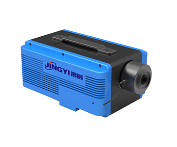
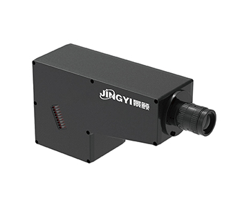
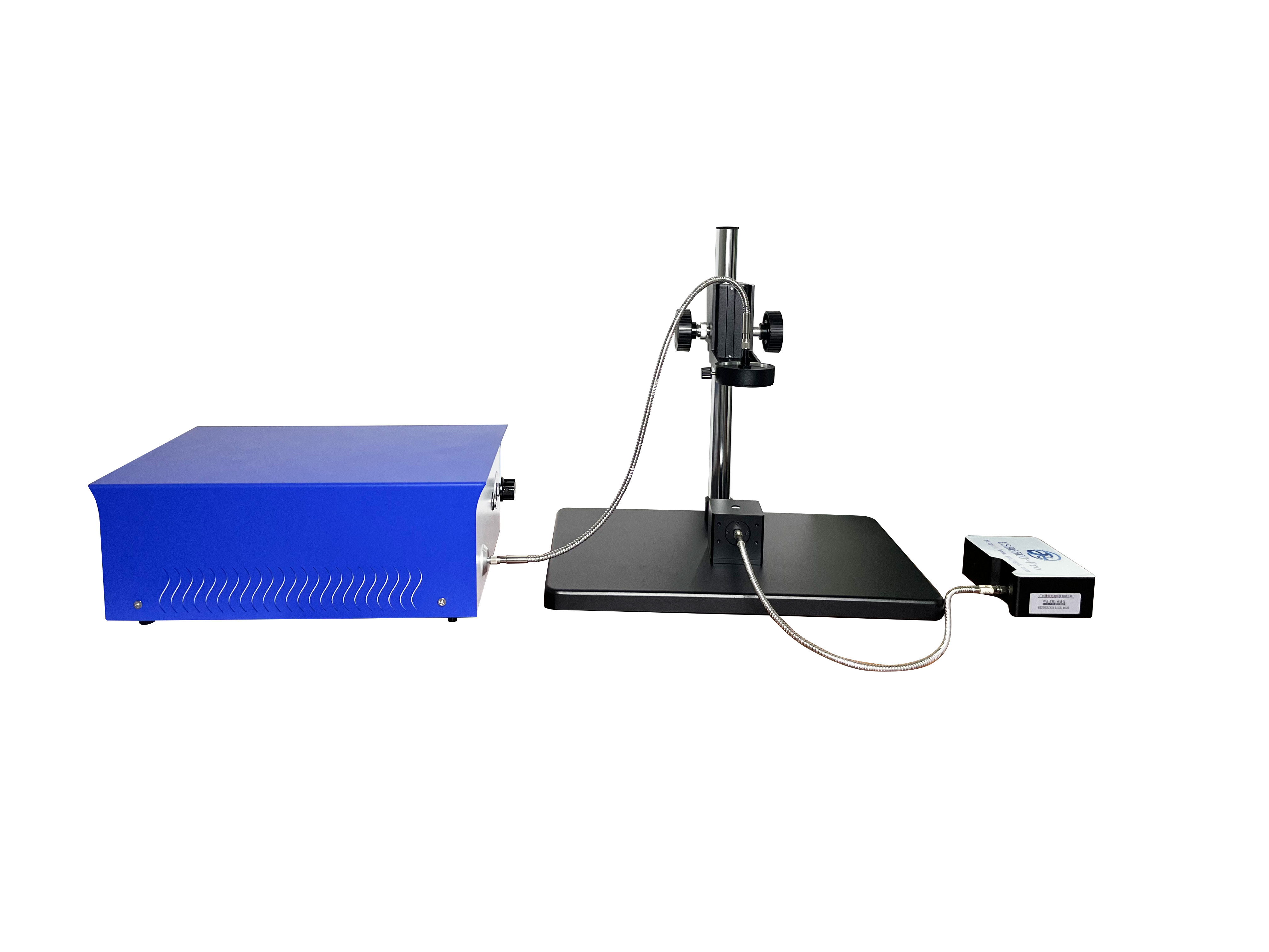
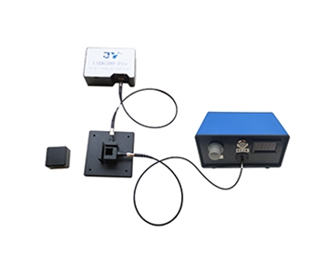
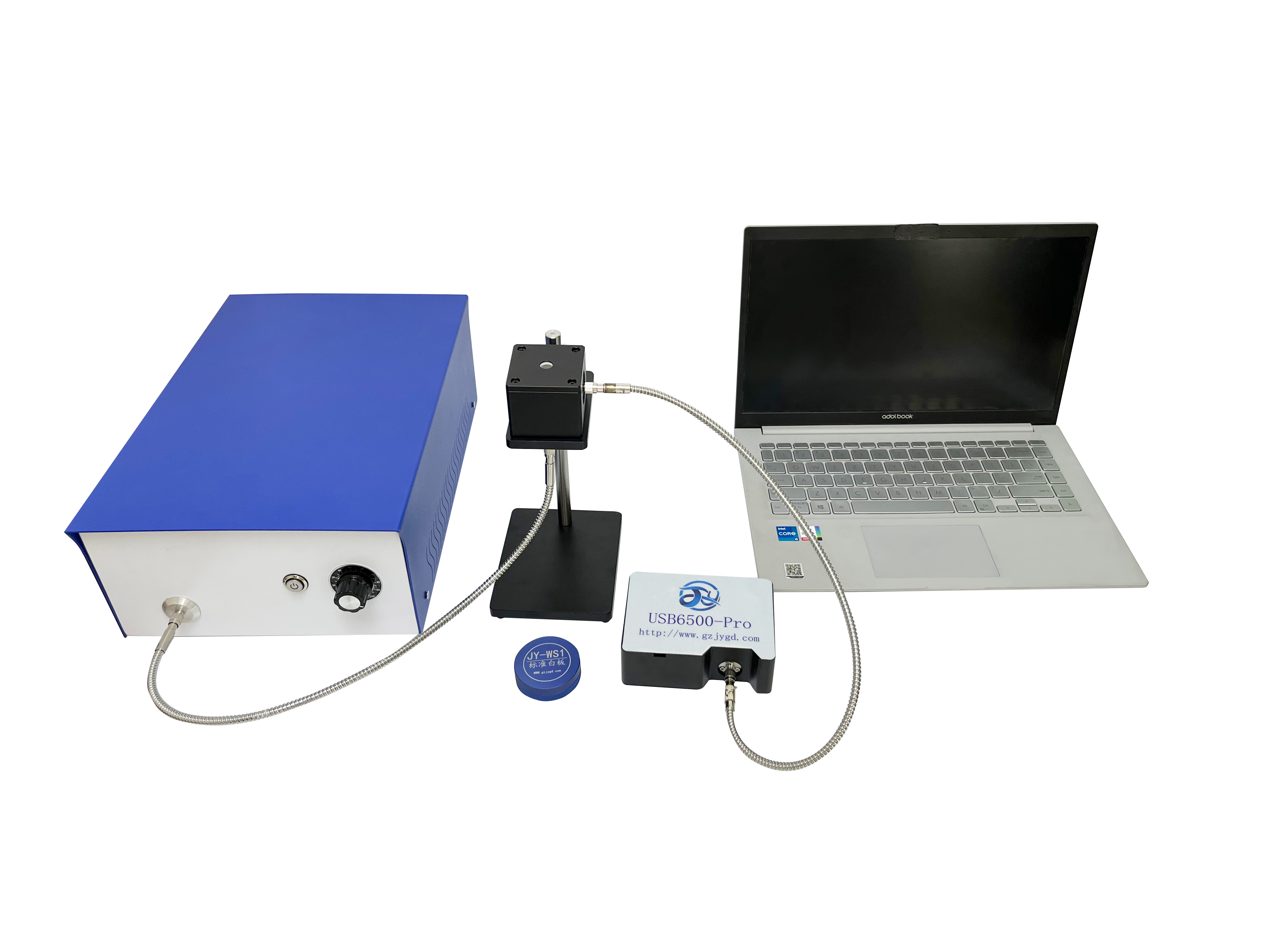
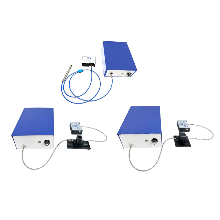
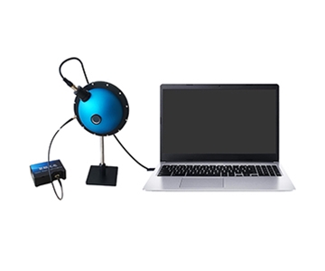
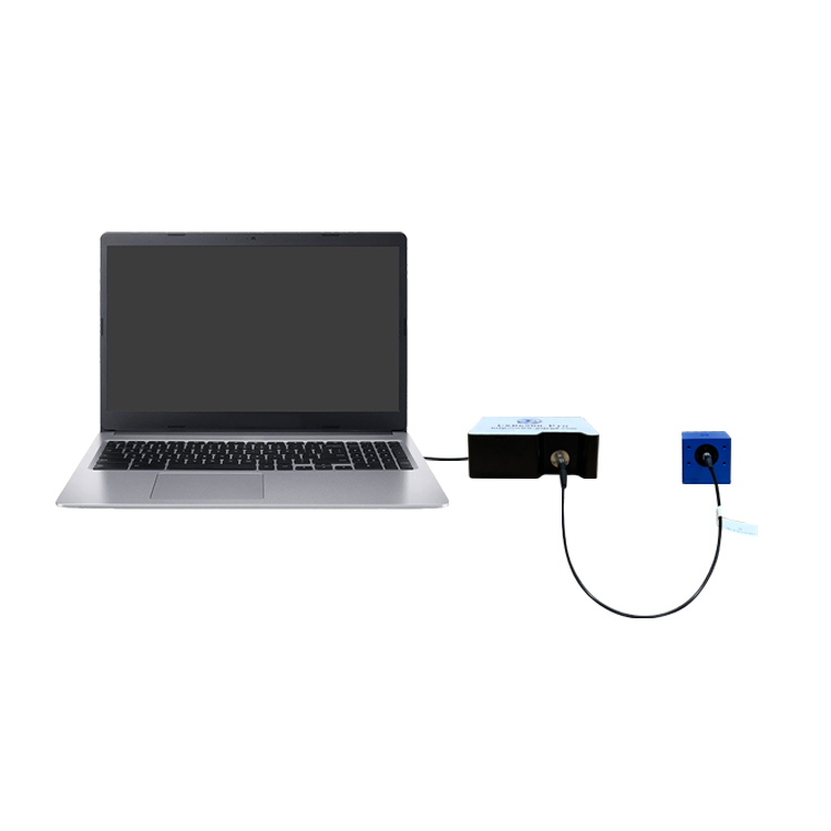
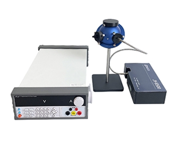
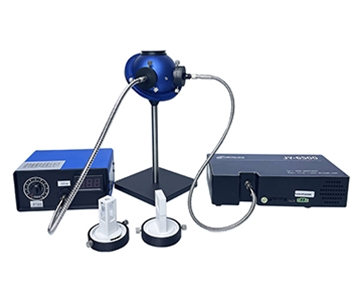
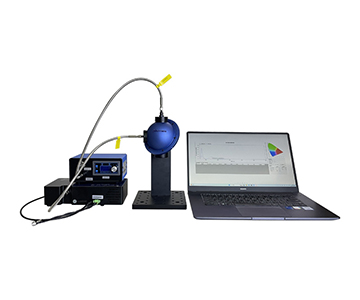
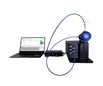
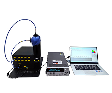
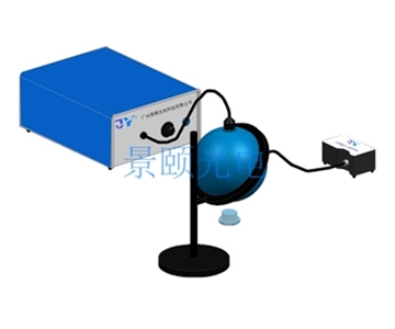
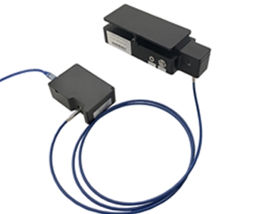
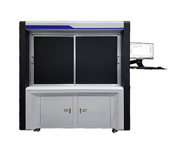
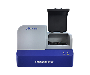
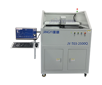
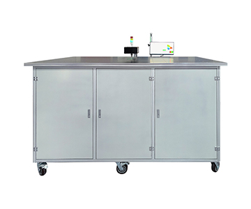
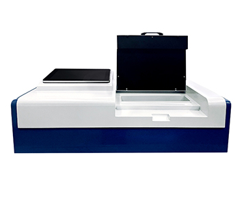
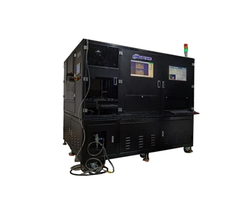
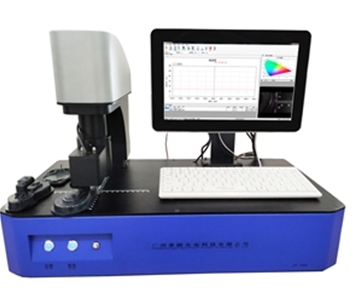
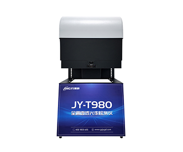
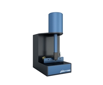
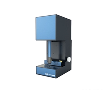
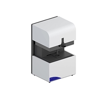
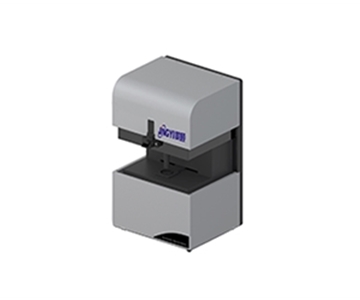
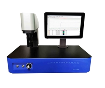
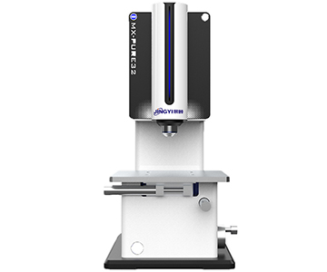
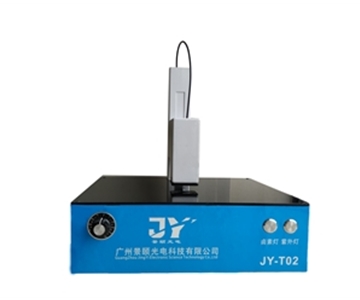
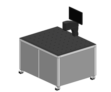
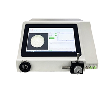
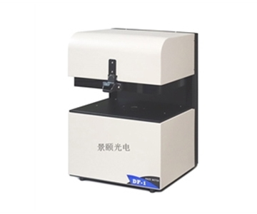
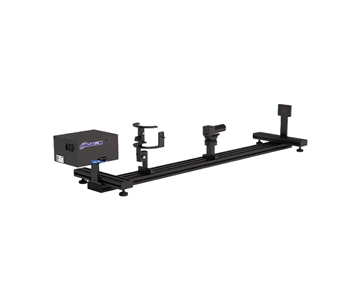
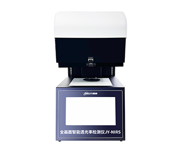
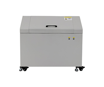
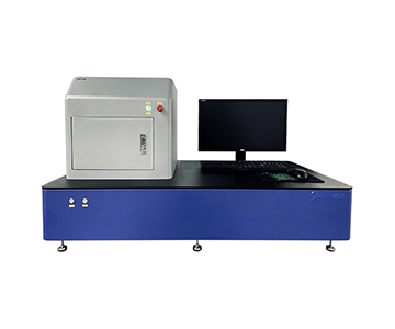
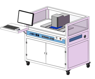
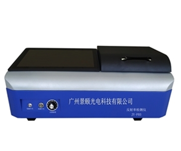
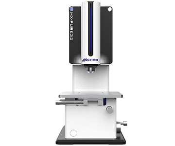
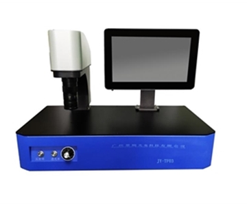
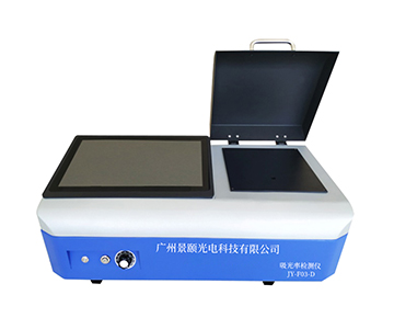
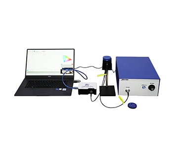
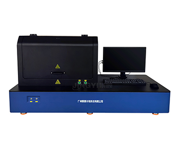
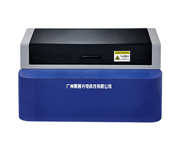
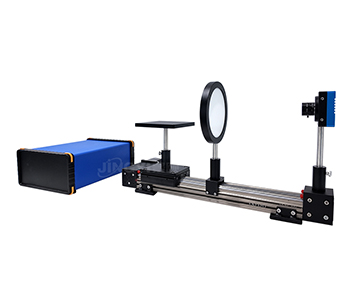
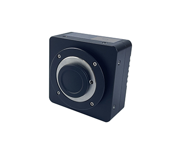
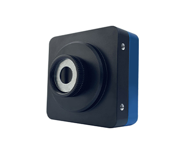
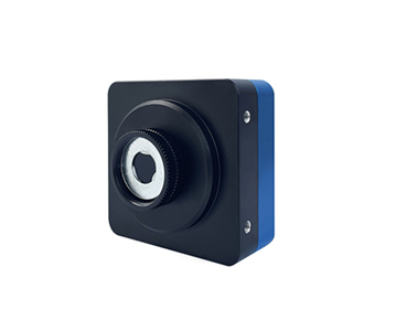
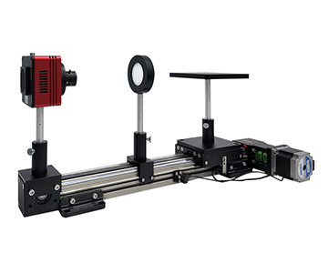
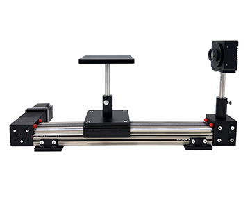
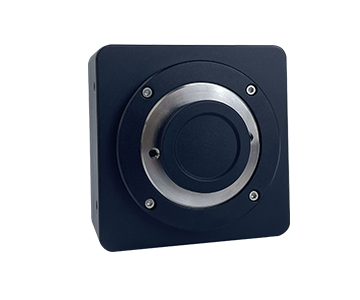
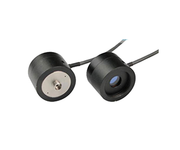
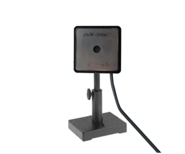
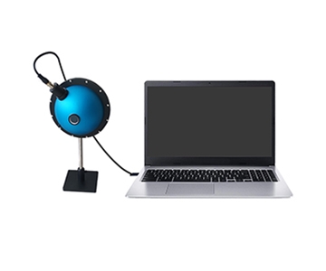
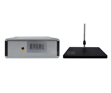
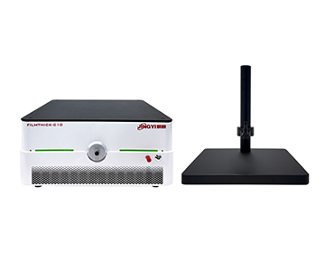
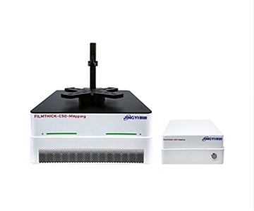
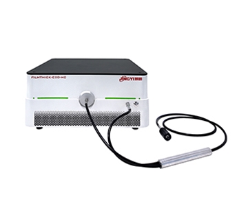
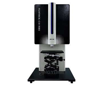
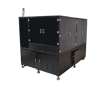
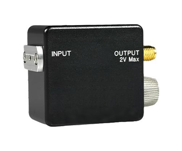
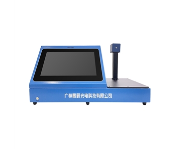
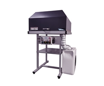
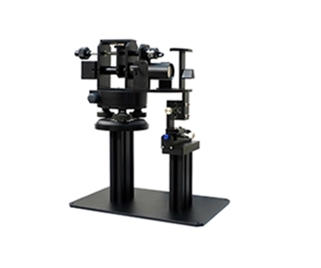
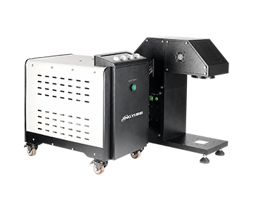
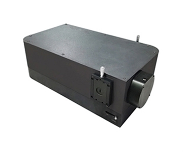
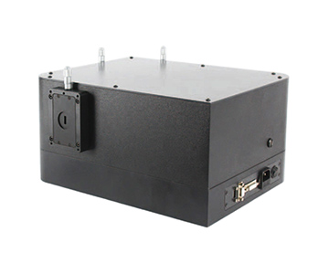
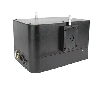
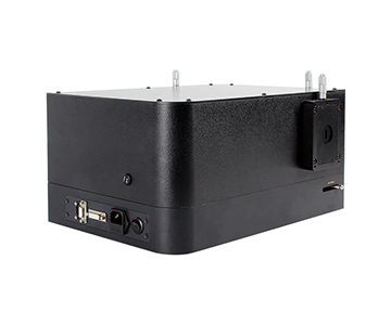
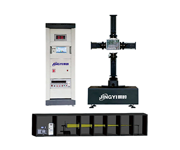
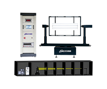
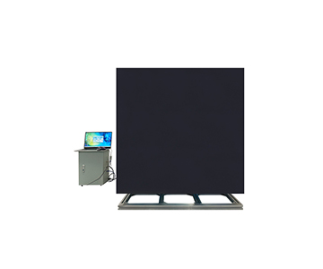
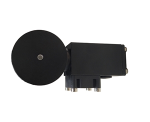
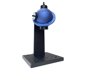
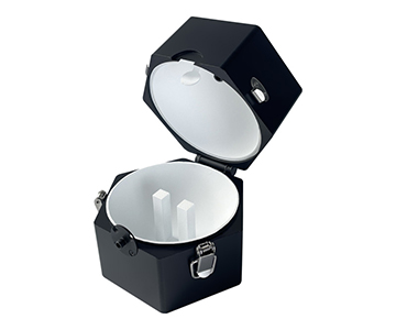
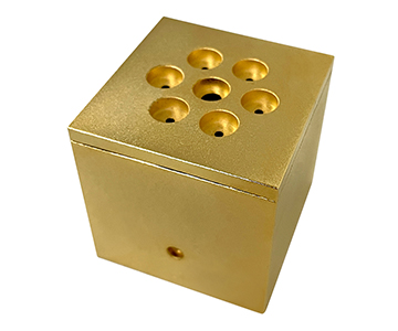
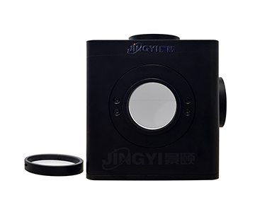
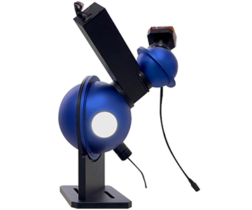
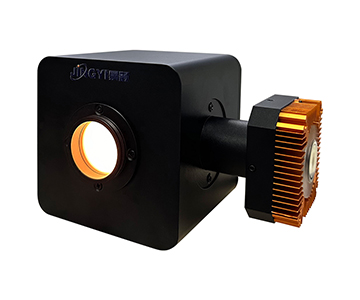
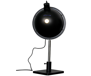
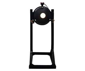
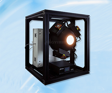
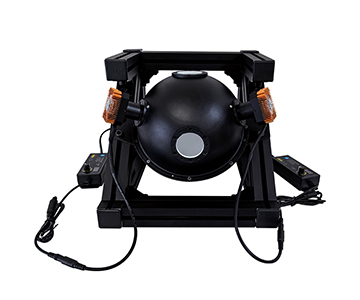
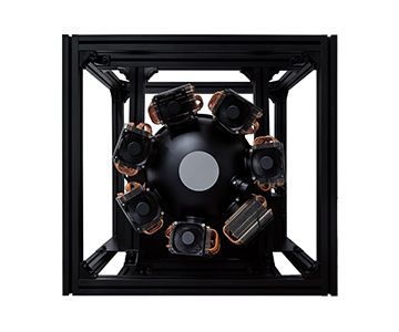
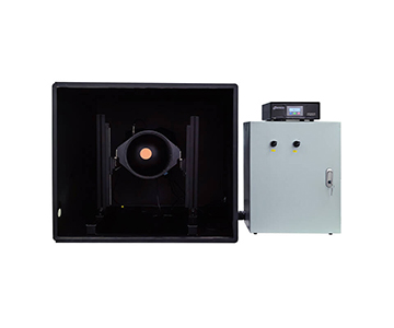
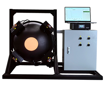
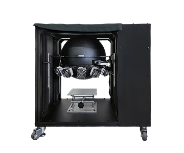
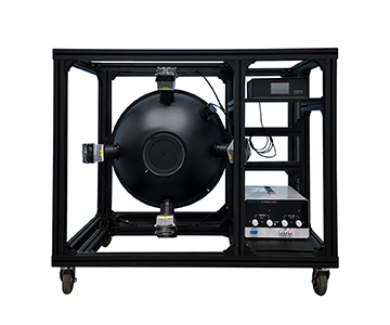
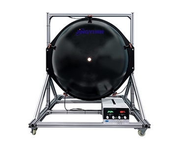
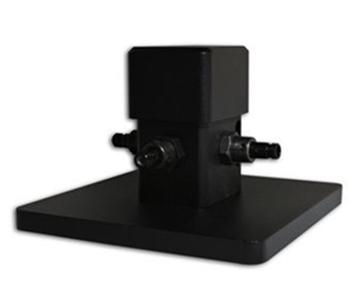
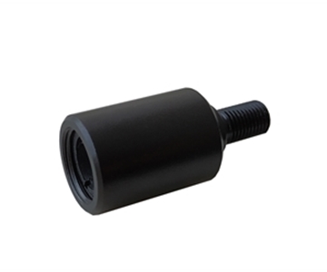
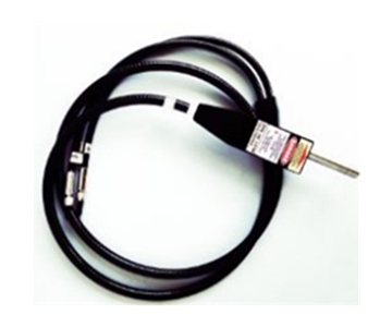
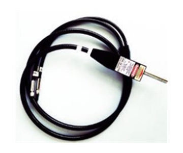
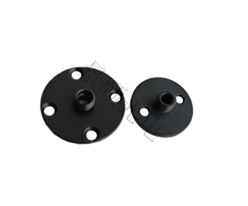
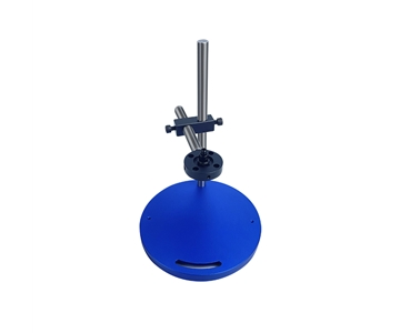
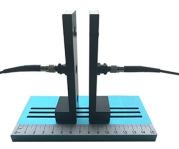
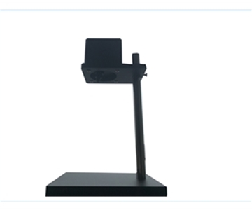
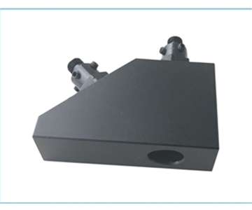
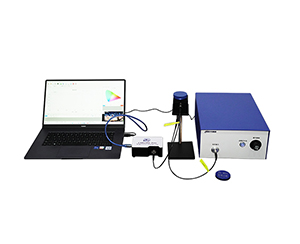
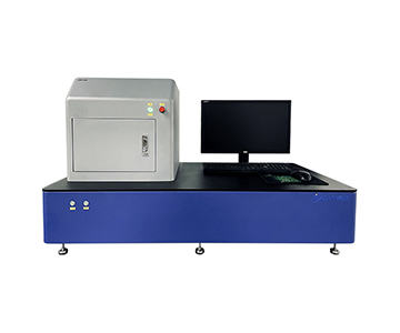
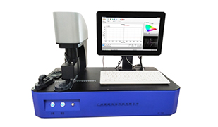
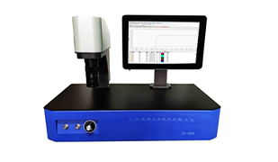
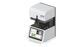
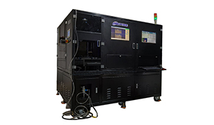
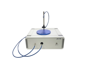
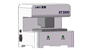
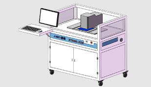
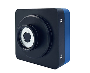
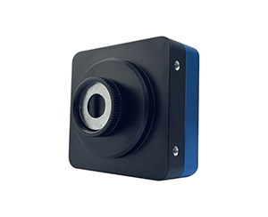
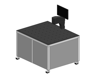
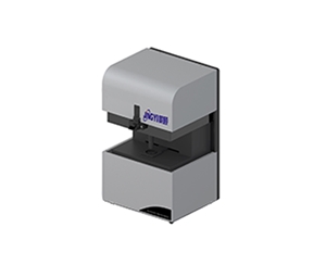
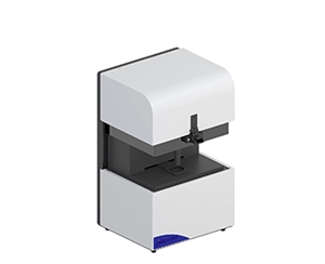
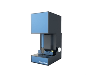
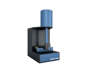
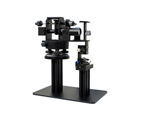
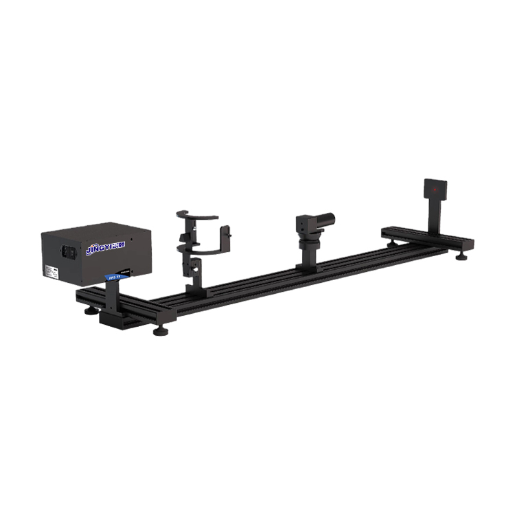
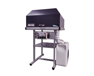
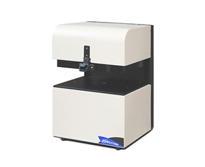
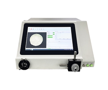
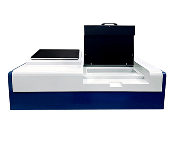
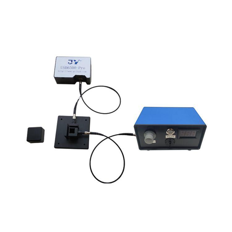
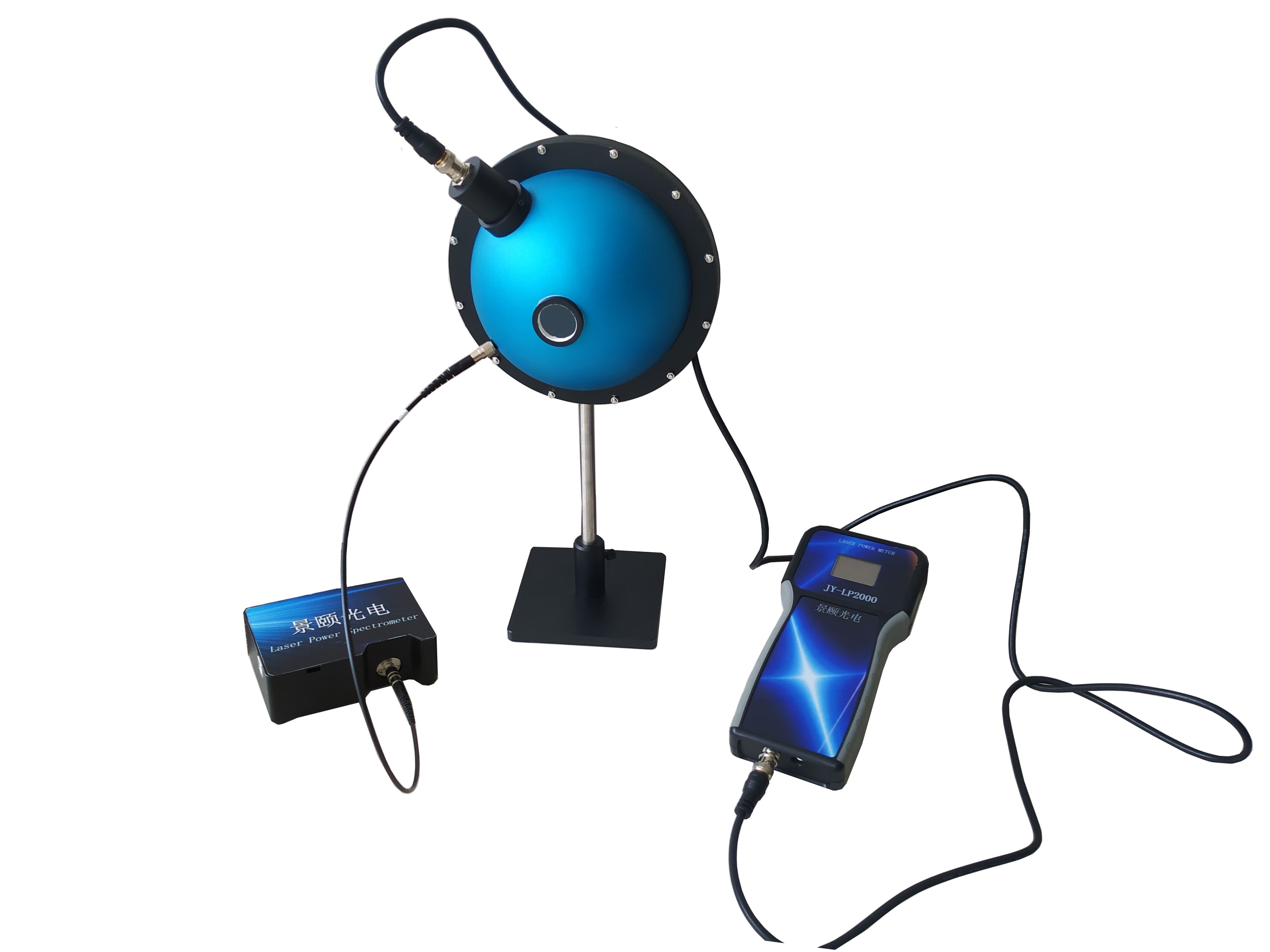
Film thickness uniformity on 2–12 inch wafers demands sub-nanometer repeatability and mapping throughput that does not bottleneck the production line. A reflective spectroscopic film thickness measurement system built on an R-Theta polar coordinate platform and a 380–1100 nm white-light interferometry engine completes 57-point full-wafer scans in 30 seconds, with single-point measurement under 0.5 seconds. Repeatability is specified at 0.2 nm, and absolute accuracy takes the greater of 0.2% or 2 nm. Three algorithms—FFT, extreme-value, and curve fitting—run in sequence to output thickness, refractive index, and extinction coefficient simultaneously. For laboratories and off-line QC in optical coating, LCD, and biomedical inspection, one unit covers 15 nm to 70 μm, eliminating instrument changeover time. Delivery lead time, however, is the variable that separates a cost-effective procurement from a hidden loss.
Define Measurement Requirements Before Discussing Models
Film stack architecture dictates the optical path. Transparent oxides, metal reflective films, single-layer photoresist, and multi-layer stacks impose completely different contrast requirements on interference fringes. For weakly absorbing films such as ITO or SiO₂, the 380–1100 nm visible band already delivers sufficient inversion signal-to-noise ratio. Thick films or near-infrared absorbing layers push the requirement toward 1700 nm.
Accuracy specifications must be split into two separate metrics. Repeatability is derived from the range of 100 consecutive measurements at the same point. Absolute accuracy is the deviation from a calibrated reference wafer. The baseline model specifies 0.2 nm repeatability on a 100 nm SiO₂/Si sample, while absolute accuracy takes the greater of 0.2% or 2 nm. Confusing these two into a single "accuracy" figure during price comparison is a frequent source of post-purchase disputes.
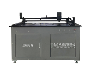
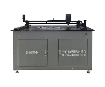
Application scenario locks the equipment form factor. Laboratory R&D prioritizes wavelength band options and multi-layer fitting. Production-line QC values cycle time and MES integration. Large flat panels or irregular substrates require an XY Cartesian platform. Mismatching scenario and form factor accounts for most equipment return and re-selection cases.
Seven Hard Specifications Breakdown (From Tested Data)
Spectral Coverage and Light Source Life
The base configuration uses a halogen-tungsten lamp. Service life is rated above 3000 hours on some models, up to 10000 hours on economy-tier units, and reaches 50000 hours on on-line thick-film versions. Wavelength starting at 380 nm covers most semiconductor thin films; extending down to 190 nm requires a deuterium lamp combination.
Spot Size and Spatial Resolution
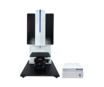
Standard spot diameter is 1.5 mm; microscope versions shrink to 60 μm or even 10 μm class. When measuring micro-zones at the edge of patterned wafers, a small spot prevents signals from adjacent film areas from mixing into the same pixel.
Single-Point Speed and Mapping Cycle
Single-point measurement is under 0.5 seconds. The polar coordinate platform is rated at 5 points in 5 seconds, 25 points in 14 seconds, and 57 points in 30 seconds. These figures directly determine in-situ dwell time per wafer.
Thickness Range and Algorithm Matching
A single base mapping unit covers 15 nm to 70 μm. FFT handles fast estimation of thick films, extreme-value method processes thin-film extrema, and curve fitting performs layer-by-layer inversion for multi-layer stacks—the three algorithms switch according to thickness magnitude.
Platform Type and Sample Size
The R-Theta polar platform accommodates 2–12 inch wafers with vacuum chuck fixation. The XY platform offers 300×300 mm travel, suitable for square and irregular substrates. Choosing the wrong platform means abandoning half the sample morphologies.
Software and Data Traceability
OPTICAFILMTEST software supports CSV, Excel, and XML export, with Manager, Operator, and Controller three-tier access permissions. As a drafting unit of T/CIET 2298-2026
Calibration Specification for Thin-Film Interferometric Thickness Measurement Systems
, the manufacturer aligns the product's repeatability data reproduced on calibrated samples with the calibration chain defined in that standard, providing an acceptance baseline.
Environmental Adaptability and Stability
Operating temperature is 18–28°C with humidity below 80% non-condensing. Film thickness stability is better than 0.05 nm—a figure that reflects long-term performance more realistically than paper-spec repeatability in shop-floor environments with air-conditioning cycling.
The most frequently overlooked combination in specification tables is "single-point time" versus "repeatability." Wafer mapping models trade a slightly larger spot for sub-second cycle time; microscope models trade longer focus time for micrometer-level landing accuracy. Focusing on only one number during procurement exposes shortcomings on the shop floor.
Candidate System Comparison Across Budget Tiers
| Tier |
Spectral Range |
Repeatability |
Typical Cycle |
Delivery & Service |
| Import Benchmark |
190–1700 nm |
Per datasheet |
Depends on distributor stock |
Lead time often exceeds 12 weeks; spare parts costly |
| Domestic Mainstream |
380–1100 nm and up |
0.2 nm |
57 points / 30 sec |
48-hour on-site service in South China; local spare parts warehouse |
| Domestic Economy |
400–1000 nm |
0.02 nm (specific samples) |
<1 sec per point |
Simplified functions; wavelength band not expandable |
The import benchmark tier holds advantages at deep-UV and near-IR extremes, but total cost of ownership must include distributor markups and downtime waiting. The domestic mainstream tier compresses delivery to within a week and supports free sampling with a repeatability report before contract signing—a weighty factor from a lead-time perspective. The economy tier fits single-film-layer QC sampling points that do not require mapping.
横向对比 shows the domestic mainstream tier's parameters within the visible band are not inferior to the import benchmark. The gap concentrates below 190 nm (deuterium lamp module) and above 1700 nm (InGaAs detector). If the production line does not involve those bands, the extra budget does not convert into yield improvement.
POC Validation: Verify Yourself, Not the Datasheet
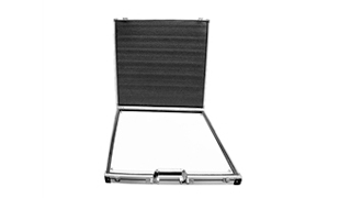
Step 1: Prepare a calibrated reference wafer.
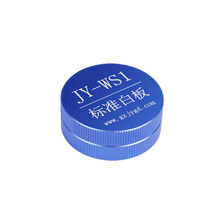
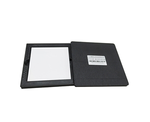
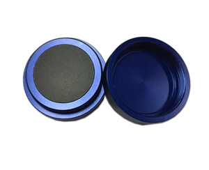
Use a supplier-provided SiO₂/Si standard sample, approximately 100 nm thick. Allow the system to warm up for 30 minutes in a 23±2°C environment.
Step 2: Run repeatability.
Measure the same location 100 consecutive times and record the range. The acceptance threshold per specification is repeatability not exceeding 0.2 nm. Exceeding this requires optical path recalibration.
Step 3: Run absolute accuracy.
Switch to an externally calibrated reference wafer (recommended with CNAS-traceable certificate). Compare measured value against nominal value; deviation takes the greater of 0.2% or 2 nm.
Step 4: Run mapping consistency.
On a wafer, select center, mid-radius (R/2), and edge points. Measure each point 5 times. Evaluate the standard deviation of the three-point mean. This step exposes radial return error of the R-Theta platform.
Step 5: Run software export check.
Confirm that the CSV output contains raw reflectance spectra, fitting residuals, refractive index n, and extinction coefficient k fields—preventing secondary development overhead when later interfacing with MES.
10-Point Pre-Procurement Checklist
1.Does the wavelength band cover both our thinnest and thickest film layers?
2.On which reference sample was repeatability measured, and can it be reproduced on our samples?
3.Does the mapping path support D-distribution and edge exclusion?
4.Is the spot size smaller than half of our minimum feature dimension?
5.Will single-point time multiplied by daily wafer count bottleneck the cycle?
6.Does the software allow an open material database, or is it locked to OEM films?
7.Is the calibration certificate CNAS-traceable?
8.What are spare part prices and lead times outside warranty?
9.Is remote diagnosis and online firmware upgrade supported?
10.Is delivery lead time written into contract pen
Among these 10 questions, item 10 is most easily glossed over by sales narratives. From a delivery-cycle perspective, an equipment delay of 4 weeks pushes the entire line's validation batch downstream—the hidden cost often exceeds the equipment price difference.
Common Engineer Selection Mistakes
Treating "accuracy" as a single number.
When a datasheet states "accuracy 0.02 nm," ask whether it means repeatability or absolute accuracy, on which sample type, and whether thermal drift is included. Many disputes originate from inconsistent definitions.
Ignoring the spot-to-feature-size ratio.
Measuring at the edge of an ITO pattern with a 1.5 mm spot pulls adjacent glass-area signals into the pixel, causing thickness underestimation. Switch to a microscope model or a reduced-spot probe.
Forcing mapping needs onto an economy-tier unit.
Economy models typically lack an R-Theta platform. Manual point programming is inefficient, and point-repeatability of only ±0.2 mm distorts full-wafer uniformity evaluation.
Overlooking the metrological traceability chain.
Confirm compliance with T/CIET 2298-2026 during selection to ensure the calibration chain from reference wafer to factory report is complete; otherwise, annual audits will issue non-conformance findings.
Objective Limitations
This solution performs strongly in the visible band and medium-to-thick film range, but two boundaries must be accepted upfront. First, the base configuration does not include 190 nm deep-UV or above-1700 nm near-IR; photoresist thin layers or thick-film silicon-based samples require band expansion modules. Second, the 0.2 nm repeatability claim is established on a thermostatic laboratory and standard SiO₂/Si samples; shop-floor temperature drift and sample roughness amplify actual range to 1.5–2× the nominal value. These are not defects but common constraints of all reflective interferometry principle equipment. Writing them into the acceptance agreement before procurement is more effective than post-delivery disputes.
Equipment Introduction Timeline Viewed from Delivery Lead Time
Split procurement into four phases: technical clarification (3–5 business days), sampling validation (including round-trip logistics, about 7–10 business days), contract and configuration lock (2–3 business days), factory release and on-site installation (subject to inventory status). Because the domestic mainstream tier maintains local spare parts warehouses and pre-installs remote diagnosis modules, sampling and installation phases typically take half the time of the import benchmark. It is advisable to write "free sampling and repeatability report before contract signing" as a precondition in the contract, avoiding discovery of excessive film-fitting residuals only after equipment arrival. Delivery lead time is not the salesperson's verbal "about 4 weeks" but a fixed number written into pen
Frequently Asked Questions
Does developer residue affect reflective interferometry when measuring photoresist thickness?
Yes. Residue
What is the core difference between on-line monitoring and benchtop models?
On-line models compress single-station response to the 0.8-second class and reserve industrial Ethernet and robotic arm interfaces. Benchtop models focus on manual stage handling and deep multi-layer fitting. Both share the same algorithm core but differ in mechanical support.
How to ensure layer-by-layer solvability on multi-layer films using optical interferometry?
It relies on curve fitting with initial guess values. More layers increase sensitivity to the material n/k database. It is advisable to require supplier permission for database editing in the contract.
How much can total cost of ownership differ between domestic mainstream and import benchmark tiers?
Beyond equipment price difference, the main gap lies in after-sales response and spare part inventory. The domestic tier offers 48-hour on-site service in South China and local consumables stock, markedly lowering downtime waiting costs.
How can I independently verify whether a supplier's claimed repeatability data is trustworthy?
Use your own SiO₂/Si sample brought to the site, measure 100 times under identical conditions without using the supplier's pre-stored data, and request a CNAS-traceable calibration certificate as an acceptance attachment.
Conclusion
Selecting a film thickness measurement system is essentially compressing four variables—accuracy, cycle time, measurement range, and delivery—into the intersection acceptable to the production line. A machine with attractive specifications but uncontrolled delivery is less worthy of a purchase order than a moderately specified machine that arrives on time.
For detailed specifications and application notes on film thickness measurement systems, search "Jingyi Optoelectronics film thickness measurement" or visit the technical library.
Reference Information
Sources
: SEMI annual reports, Chinese Optical Society technical white papers, customer-authorized validation data, T/CIET 2298-2026
Calibration Specification for Thin-Film Interferometric Thickness Measurement Systems
Author
: Cai Xiaodong, Senior Application Engineer, Jingyi Optoelectronics — 12 years in optical metrology and industrial precision measurement equipment
Conflict of Interest
: Jingyi Optoelectronics manufactures film thickness measurement systems. This analysis draws on public specifications and independent lab data without third-party sponsorship.
Intended Use
: Educational reference only; validate all equipment choices through on-site POC testing under your specific process conditions.
Updated
: October 2026