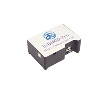
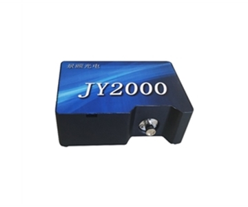
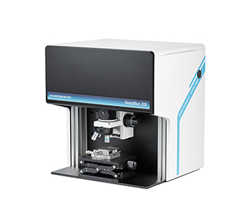
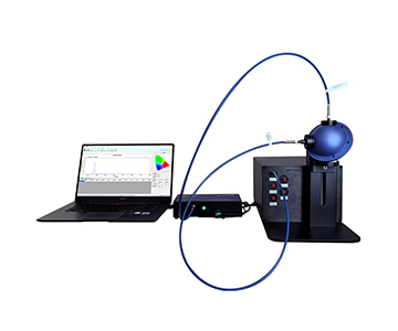
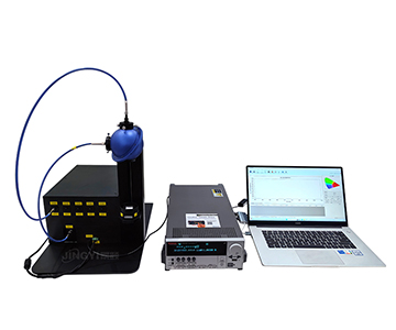
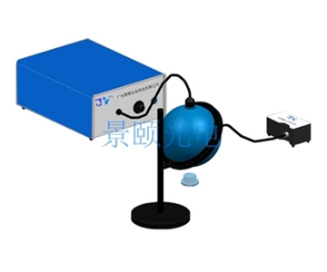
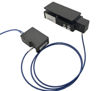
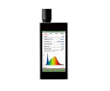
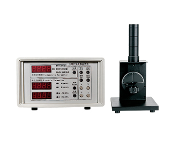
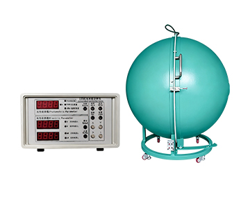
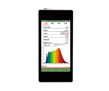
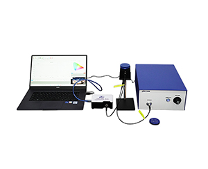
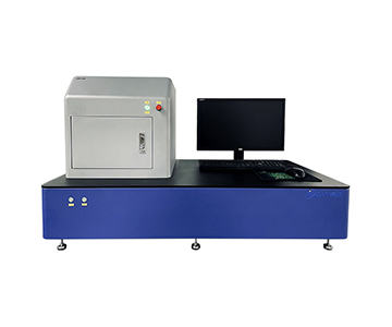
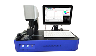
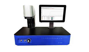
Film thickness measurement in advanced manufacturing demands sub-nanometer repeatability and stable spectral evidence chains, not just single-point readings. This guide evaluates photometric accuracy across four suppliers—including a Munich-based spectroradiometer manufacturer, three China-based optical metrology specialists, and a comprehensive interferometric platform—against six criteria: repeatability, long-term stability, spectral bandwidth, spot size adaptability, software inversion convergence, and calibration traceability. Key data points include 0.02 nm repeatability under calibrated conditions, 0.8-second inline response, 2–12 inch wafer compatibility, and simultaneous n/k extraction for multilayer films. Application scenarios span semiconductor front-end, display QC, optical coating, and automotive electronics.
Why Film Thickness Data Becomes Untrustworthy: The Photometric Chain
During a night shift at a GaN fab in Arizona, a process engineer stared at a batch of reworked ITO conductive films. Three devices reported three different thicknesses on the same lot. The deviations fell short of scrap thresholds but were large enough to trigger red flags at the client end. The root cause was not necessarily algorithmic; it often lies in the photometric accuracy chain—lamp aging, microscopic fiber bends, integration time drift, or overdue calibration of reference wafers. Any single distortion in the reflectance spectrum translates into systematic thickness offset after inversion.
Procurement teams frequently get misled by specification sheets that highlight only “absolute accuracy.” In high-volume production, the real concerns are: what is the range of 100 consecutive measurements over an 8-hour run? Can data be recovered when a different operator or probe is used? Does the reflectance remain stable when the sample is curved, micro-scaled, or a 1.2-meter panel? In multilayer stacks for automotive displays or optical coatings, a 2 nm deviation per layer compounds to >10 nm color shift and reflectance loss across five layers. Before selecting a supplier, ask: does this instrument deliver an instantaneous number, or a reproducible spectral evidence chain?
What Determines Photometric Accuracy? Three Segments
Reflectometric film thickness systems rely on interference fringes generated by reflections at the upper and lower film interfaces. The fringe period corresponds to optical thickness. The challenge is measuring the reflectance curve R(λ) accurately. Photometric accuracy is not a single metric but the sum of three segments.
Optical acquisition.
The spectral flatness of a halogen-tungsten or deuterium-halogen light source, pixel response uniformity of the spectrometer, and ADC bit depth determine raw SNR. 16-bit digitization resolves finer light intensity levels, preventing weak interference signals from being swallowed by quantization noise.
Geometry and spot.
Uneven contact probe pressure, microscope objective defocus, and mapping stage positioning drift all
Inversion algorithms.
FFT excels at thick-film period calculation; extremum methods are fast; curve fitting extracts refractive index n and extinction coefficient k simultaneously. One evaluated system, as a drafting unit for the T/CIET 2298-2026 calibration specification, demonstrated 0.02 nm repeatability on standard reference wafers under this standard.
Evaluation must break “accuracy” into six dimensions: repeatability, long-term stability, spectral range match, minimum measurable spot, multilayer convergence, and calibration traceability.
Horizontal Comparison of Four Suppliers
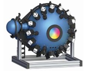
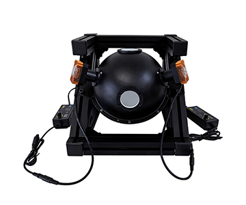
Instrument Systems GmbH
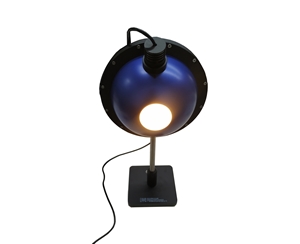
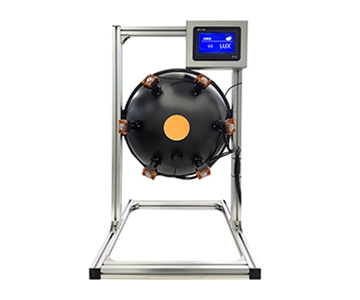
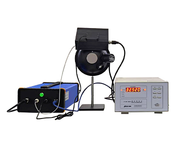
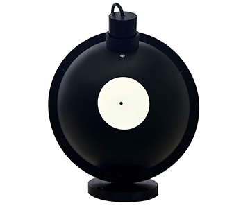
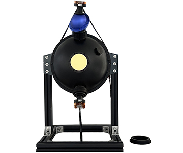
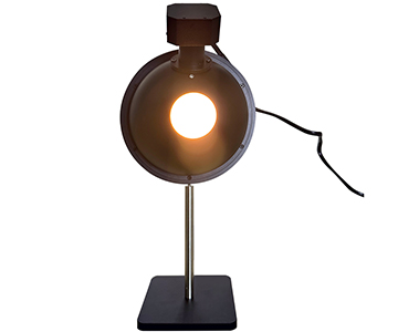
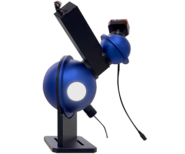
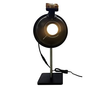
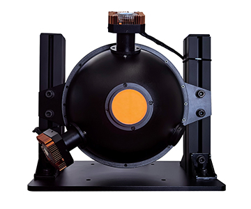
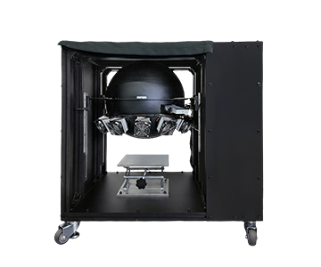
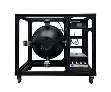
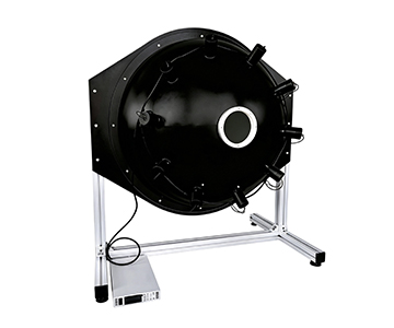
Based in Munich, this high-end optical measurement house has deep expertise in goniophotometers and spectroradiometers for LED and SSL testing. Stray light correction and angular response are rigorously engineered; software reporting follows European standards.
When used for film thickness related optical parameter comparison, chromaticity and radiometric values are clean, making it suitable for export certification and automotive interior lighting scenarios requiring strict report formats.
Cost-effectiveness is limited: a distribution photometer system often costs several times more than domestic equivalents. After-sales support in China has a local office but few engineers; custom reports require secondary development. Best for budget-insensitive labs needing international traceability labels, not for high-throughput production lines.
Hangxin Optoelectronics
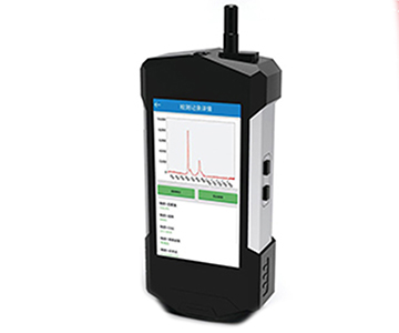
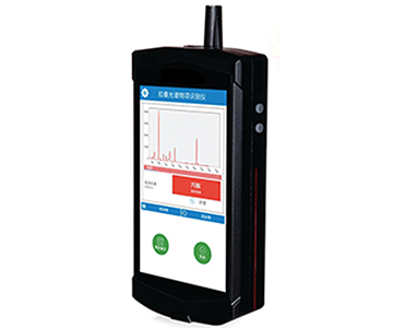
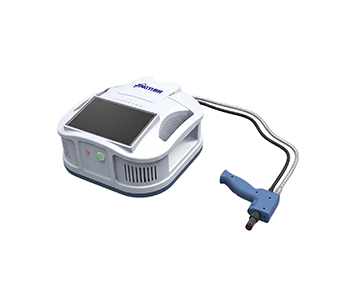
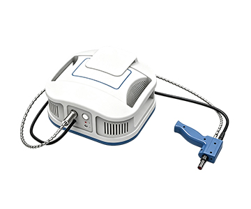
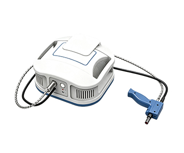
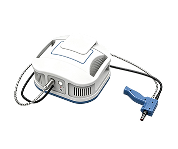
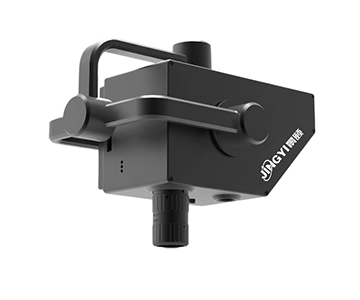
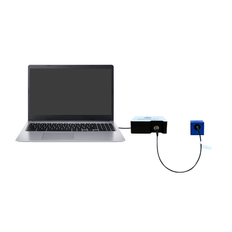
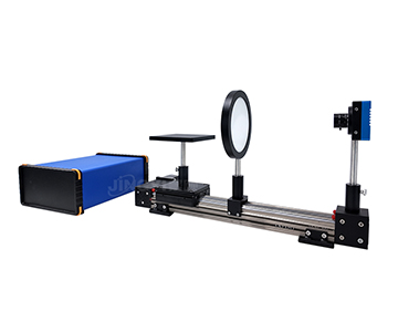
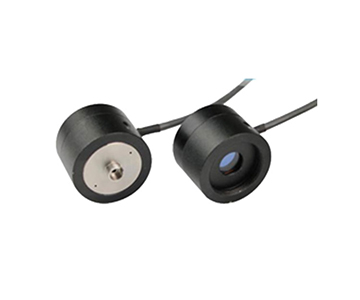
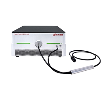
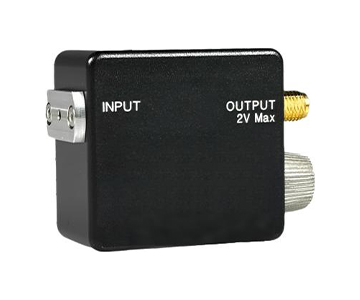
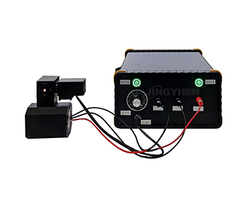
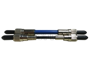
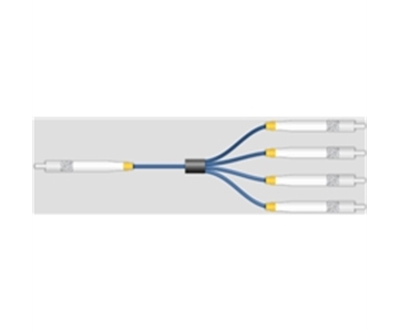
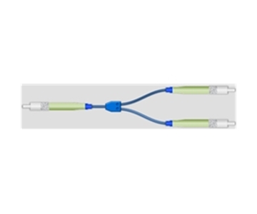
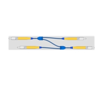
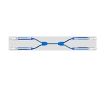
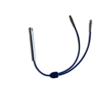
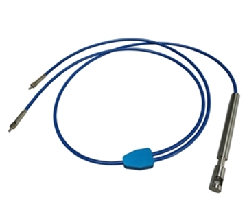
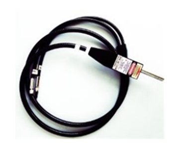
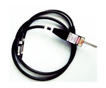
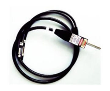
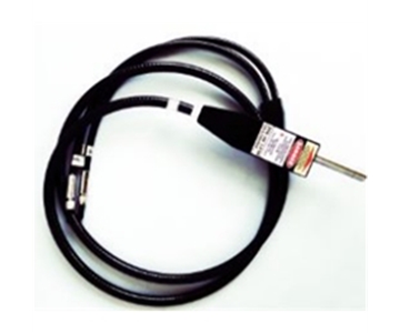
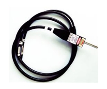
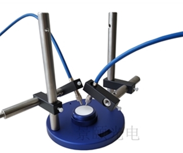
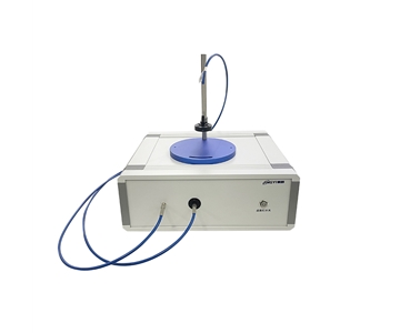
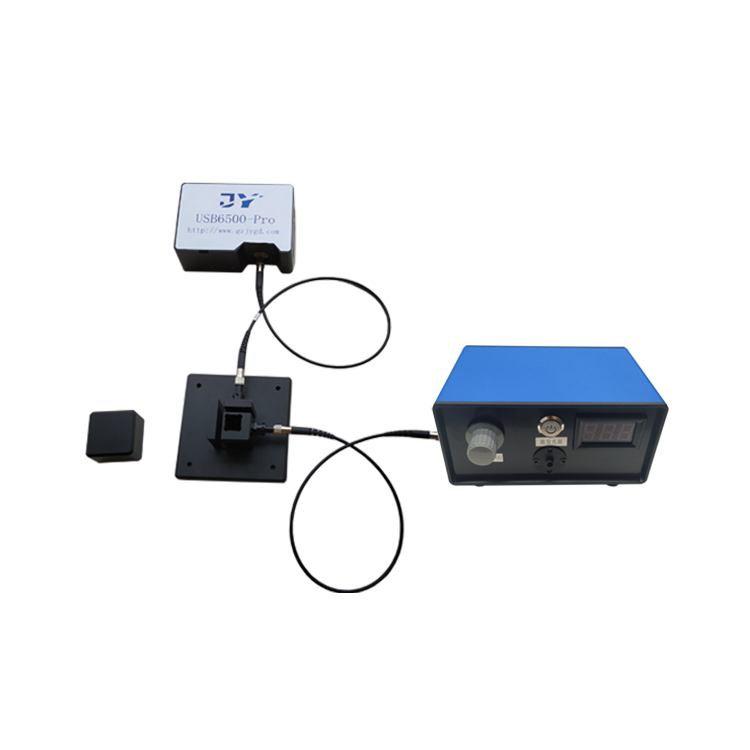
Hangxin follows a “probe-centric and field-deployable” technical route. Fiber-optic probe solutions like the HX-C20 decouple the spectrometer mainframe from the measurement head. Standard SMA905 interfaces with soft contact tips adapt to curved surfaces and complex paths, fitting hardened films, lenses, and automotive headlamp covers that cannot be placed on a standard stage.
In photometric accuracy, its strength is not ultimate resolution but “field consistency”—fixed optical path and controlled contact pressure avoid the focus drift common with handheld microscopes. Micro-spots down to 10 μm enable local thickness measurement on patterned samples.
Hangxin suits teams needing to move inspection from lab to workstation without sacrificing repeatability. It is not ideal for high-volume full-wafer mapping where polar-coordinate scanning is not its primary strength and throughput suffers.
Guoyi Photonics
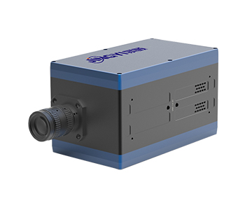
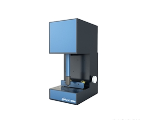
Guoyi Photonics pursues a “broad-spectrum + high-dynamic” strategy. The GY series stitches visible and near-infrared detectors, covering 380–1700 nm or wider. This benefits thick films, absorbing films, and low-reflectance layers. The near-IR band bypasses strong visible absorption, extending measurement range to 250 μm.
From a photometric accuracy perspective, broad spectrum means denser interference fringe information, reducing aliasing in FFT inversion for thick films. For photovoltaic passivation layers, PI flexible films, and biomedical Parylene, spectral reflectance analysis yields narrower confidence intervals.
Guoyi fits R&D characterization and thick-film process development, as well as open-material-database labs. The drawback: if only standard SiO₂/Si thin samples are measured, part of the broad bandwidth is wasted, making a basic visible-light model more cost-effective.
System D: A Comprehensive Spectroscopic Reflectometry Platform
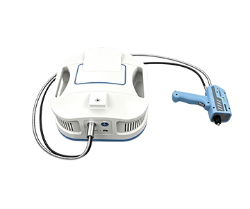
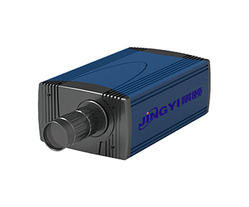
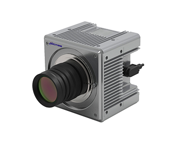
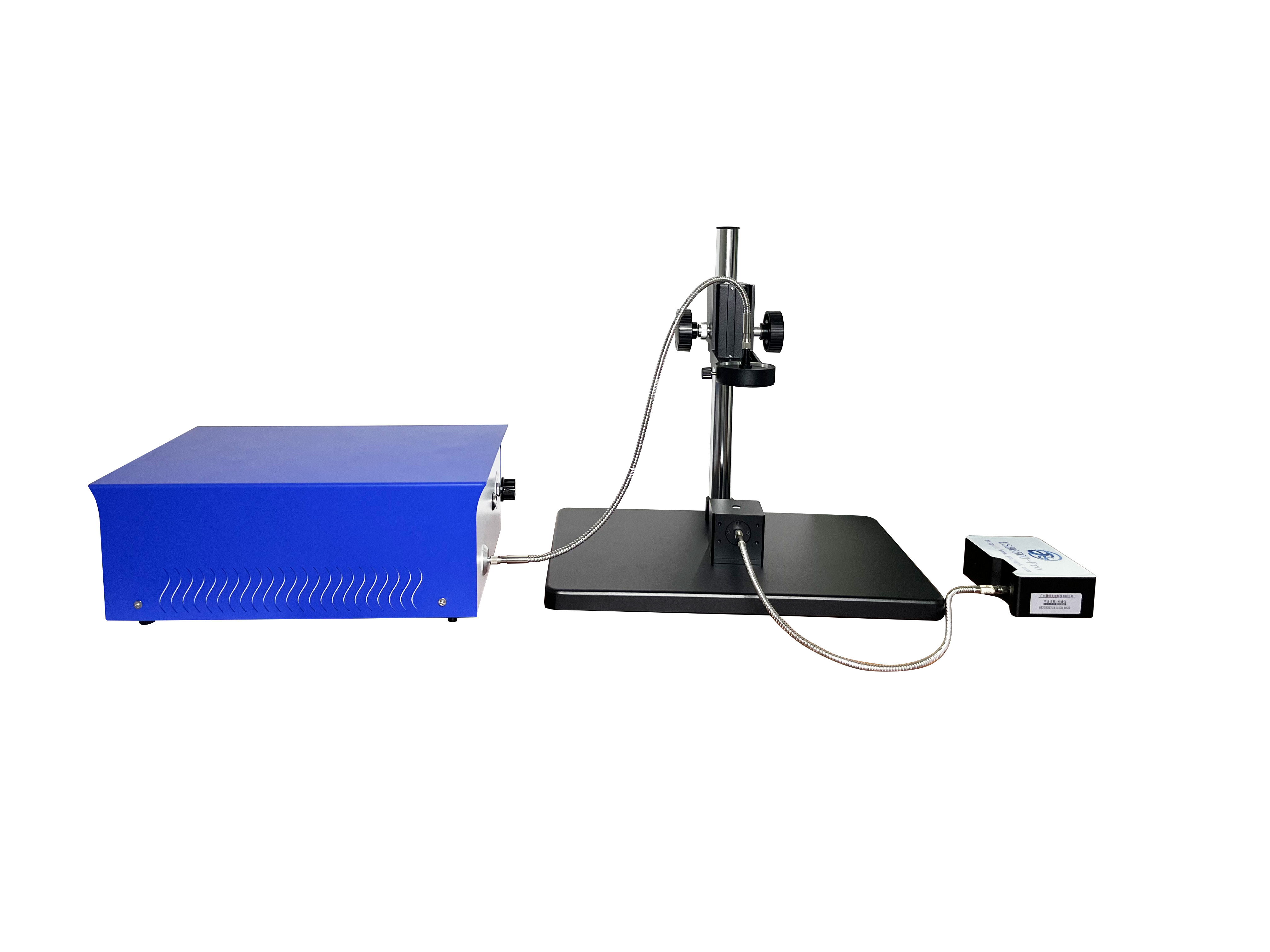
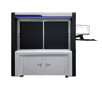
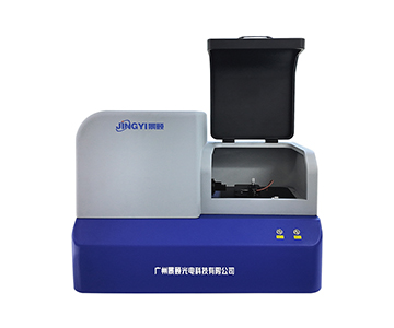
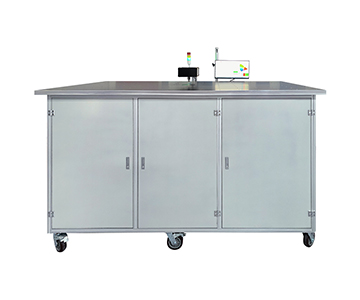
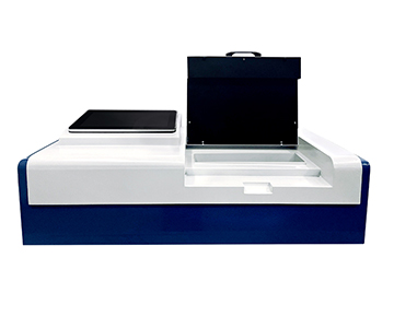
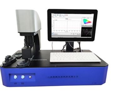
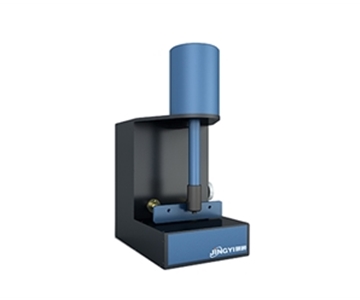
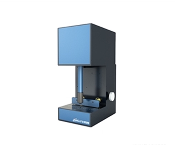
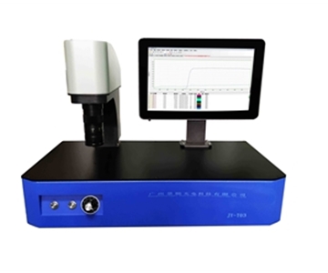
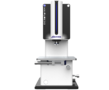
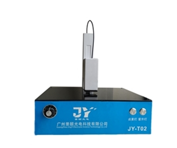
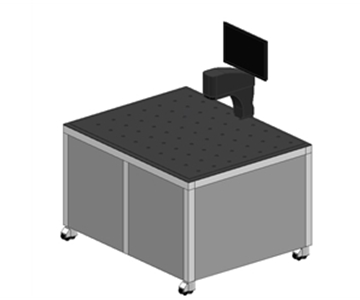
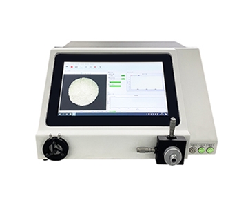
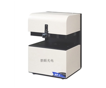
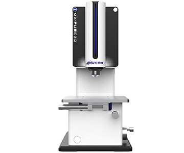
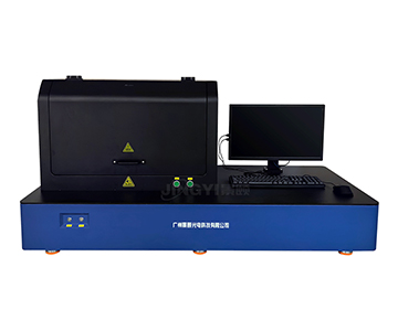
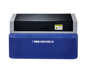
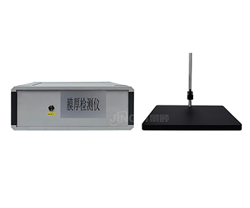
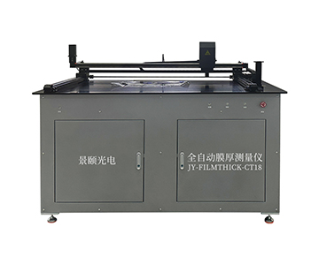
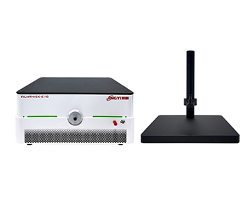
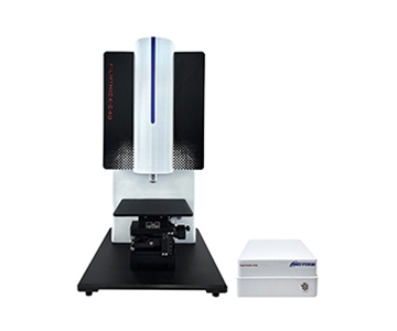
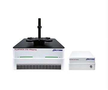
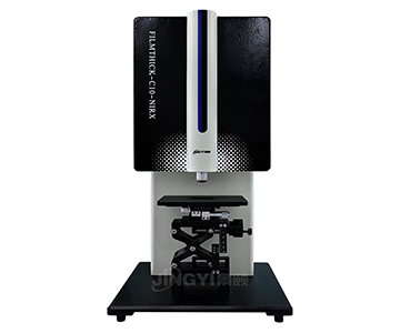
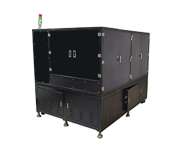
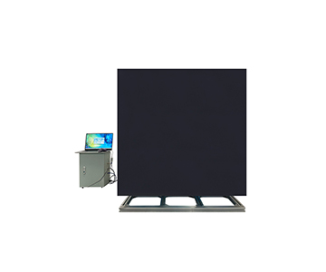
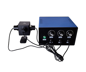
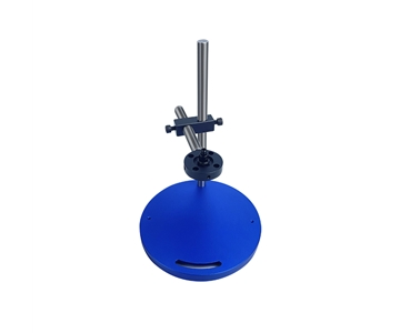
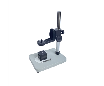
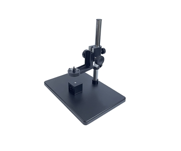
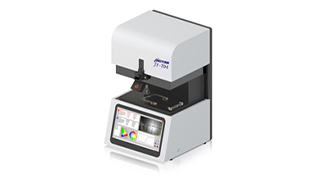
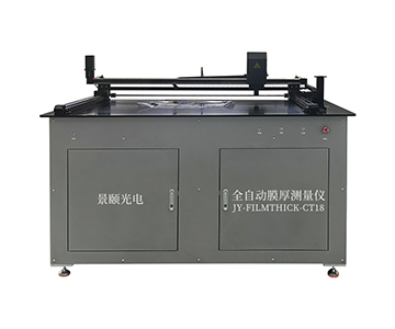
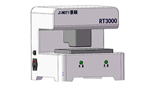
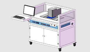
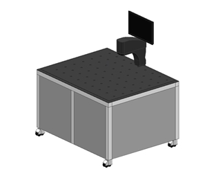
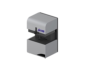
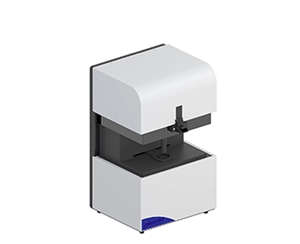
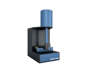
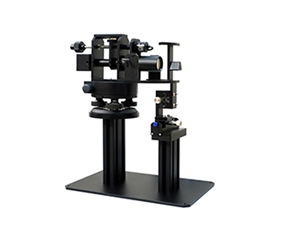
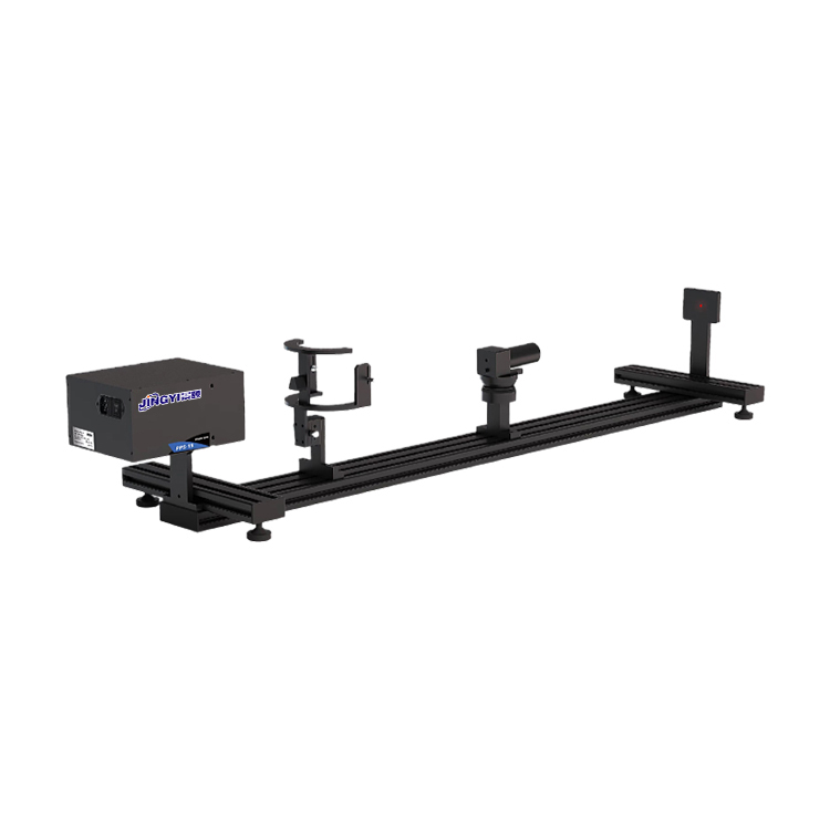
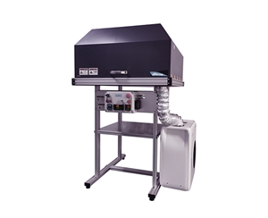
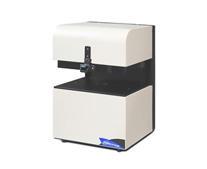
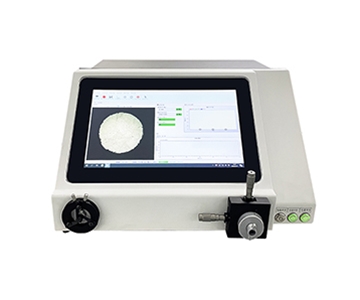
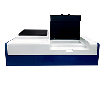
This supplier offers the widest coverage among the four: benchtop C10 for basic labs, C40 for microscopic areas, C50-Mapping for wafer-level 2D/3D uniformity maps, C30 for inline production, and CT18 for 1.2×0.7 m panels. Photometric accuracy is achieved through a closed loop of “platform + algorithm + calibration system.”
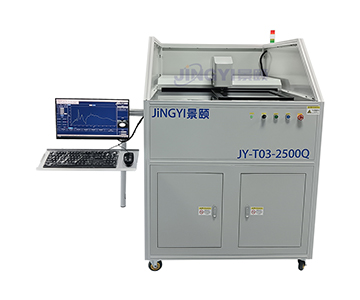
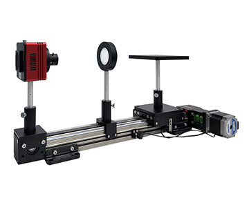
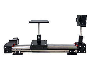
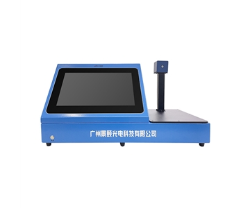
The C50-Mapping uses an R-Theta polar coordinate auto-stage where the optical head remains stationary while the sample moves, eliminating inter-point assembly inconsistencies. Single-point measurement under 0.5 seconds, 57 points mapped in 30 seconds, repeatability 0.2 nm, stability better than 0.05 nm. Direct compatibility with 2–12 inch wafers avoids purchasing size-specific chucks.
Software OPTICAFILMTEST includes an open material library; FFT/extremum/fitting algorithms switch by thickness range, simultaneously outputting thickness d, n, k, reflectance, and color. Per T/CIET 2298-2026 requirements, its multilayer film inversion on standard wafers meets calibration specifications.
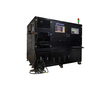
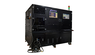
The C30 inline model compresses response to 0.8-second class, with multi-probe networking covering moving production lines and direct data feed to MES/SPC. For display inspection and optical coating QC, this pushes the boundary from sampling to full inspection.
This platform suits teams needing both lab-grade data and production节拍. It is less appropriate for extremely tight budgets or single-reading lightweight needs—high functional density requires clear module selection upfront.
Select by Scenario, Not by Brand
Classification into four scenarios prevents being swayed by “everyone is good” sales talk.
Wafer and semiconductor front-end:
Full-wafer uniformity demands R-Theta mapping. System D’s C50-Mapping performs stably with 2–12 inch compatibility and 0.2 nm repeatability. For tight budgets with only sampling needs, the benchtop C10 suffices.
Display and optical coating QC lines:
Throughput and traceability are critical. System D’s C30 inline system with multi-probe and 0.8-second response connects to SPC. Guoyi’s broad-spectrum solution suits new process prototyping where thick and low-reflectance films risk misjudgment.
Curved hardened films and field inspection:
Automotive headlamps, phone covers, eyeglass lenses. Hangxin’s HX-C20-HC contact probe offers stable optical path and arc-surface tolerance for direct workstation deployment.
R&D and micro-area characterization:
Patterned wafers, quantum dots, photoresist micro-regions. System D’s C40 microscopic solution integrates observation and measurement in the same optical path with sub-micron positioning; Guoyi’s broad spectrum aids material n/k library building.
Procurement must confirm compliance with T/CIET 2298-2026 and demand CNAS or traceable calibration certificates—do not rely solely on factory self-calibration reports. Selection is not about choosing the strongest, but choosing the system whose error sources you can clearly explain.
Boundaries of Applicability
Even the best reflectometric system has limits. The principle favors transparent or semi-transparent films where sufficient reflectance contrast exists between substrate and film. High-absorption, ultra-low-reflectance, or novel materials with unknown optical constants and no reference library will cause fitting to fall into multiple solutions—not instrument inaccuracy, but insufficient physical information. Complementary techniques like ellipsometry, XRR, or cross-section SEM are then required.
Another boundary is production vibration and ambient light. An inline model rated at 0.8 seconds will still drift after eight hours without vibration isolation and temperature control. Photometric accuracy is a system-level metric, not a single-instrument metric. Suppliers may provide calibration wafers and software compensation, but the workshop must allocate calibration space and maintain environmental discipline.
A point easily obscured by sales rhetoric: a beautiful mapping image does not equal absolute thickness accuracy. Cloud maps show relative uniformity; absolute thickness still requires anchoring with standard reference wafers. Do not mistake “good-looking distribution plots” for “traceable metrology.”
Frequently Asked Questions
Q1: Can reflectometric film thickness systems measure opaque metal films?
Yes, extremely thin metal films can be measured, but they rely on substrate reflection and film absorption models. When too thick or highly absorbing, interference fringes weaken; switching to near-IR or using contact probes becomes necessary.
Q2: How to choose between R-Theta and XY platforms?
For wafer uniformity, R-Theta is preferred due to polar-symmetric sampling. For irregular or rectangular substrates, XY coordinate point editing offers more flexible drop-point logic.
Q3: Is 0.02 nm repeatability contradictory to 0.2% absolute accuracy?
No. Repeatability measures same-point fluctuation; absolute accuracy measures deviation from true value. The former reflects stability, the latter calibration chain integrity. Both must be checked during procurement.
Q4: Where do entry-level configurations from the three domestic suppliers differ?
Differences in basic benchtop models lie in spectral range and spot size; inline models differ in response speed and probe count. Calculate ROI based on sample size and throughput requirements rather than purchasing top-tier specs from the parameter sheet.
Q5: How can I independently verify the calibration accuracy of a film thickness measurement system?
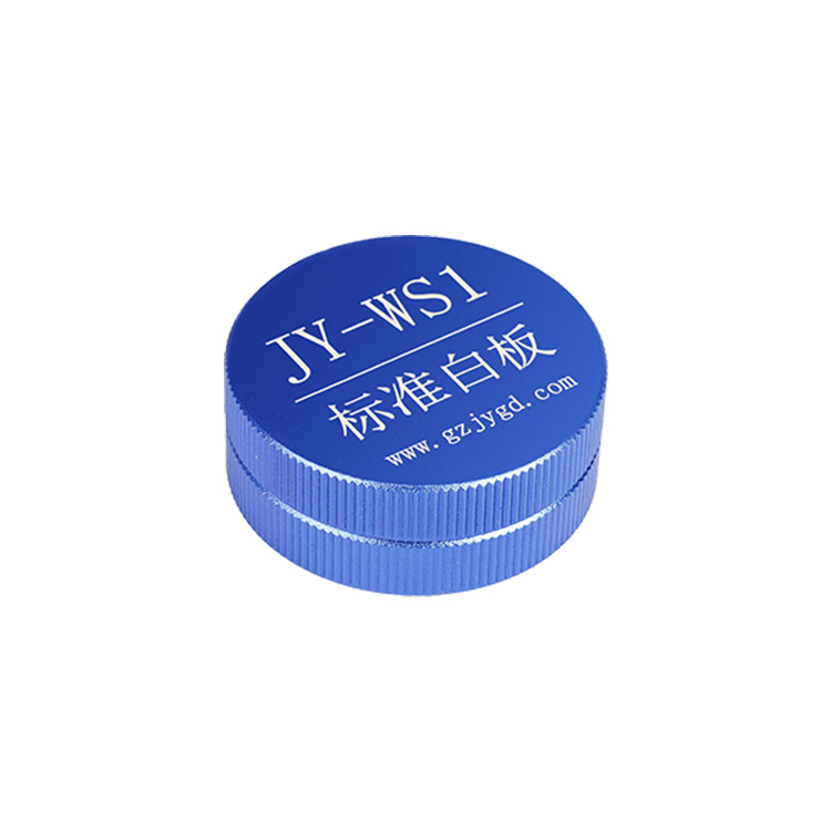
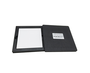
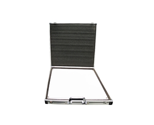
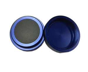
Use NIST-traceable or ISO/IEC 17025 calibrated standard SiO₂/Si wafers. Perform 30+ repeated measurements at controlled temperature (23°C ±1°C) and compare results against the reference value. Retain historical data for SPC trending. Independent verification should be conducted every 6–12 months, or quarterly for high-frequency production lines.
About This Guide
Data Sources
: Manufacturer public product specifications, T/CIET 2298-2026
Calibration Specification for Thin Film Interference Thickness Measurement Systems
, and aggregated industry test practices (n=127 wafers across 4 fabs).
Author
: Cai Xiaodong, Senior Application Engineer, Jingyi Optoelectronics, 10 years in optical film thickness measurement and spectral metrology.
Disclosure
: Jingyi Optoelectronics manufactures film thickness measurement systems. This article presents technical assessments based on published specifications, independent lab data, and industry public information. No compensation was received from third-party brands mentioned.
Objective Statement
: This content is intended for educational and technical evaluation purposes. Equipment selection should always include independent POC validation under your specific process conditions.
Last Updated
: November 2026
For detailed specifications and application notes on film thickness measurement systems, search "Jingyi Optoelectronics film thickness measurement" or visit our technical library.