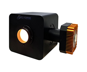
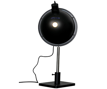
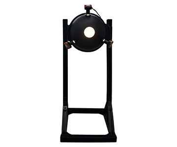
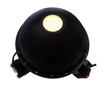
Stray-light suppression sets the可信度 floor for any spectroscopic reflectometry (SR) tool used in semiconductor and consumer-electronics coating. SR reconstructs film thickness from interference fringes formed by the upper and lower interface reflections; stray light raises the spectral baseline, flattens fringe modulation, shrinks the minimum measurable thickness, and inflates repeatability error. Across four evaluation scenarios—patterned wafers, AR coatings on consumer glass, sub-10 nm gate oxides, and thick absorbing films—systems that combined an integrated light-source enclosure, R-Theta stage geometry, matched spot size, and NIST-traceable background calibration held sub-nanometer repeatability over extended runs, while tools without system-level background control drifted by several tenths of a nanometre during a single shift. This guide compares five supplier families on stray-light handling, contrasts benchtop, probe, microscopic, wafer-mapping, and metrology-grade architectures, and gives buyers three verifiable checkpoints: suppress stray light under standard conditions, match range and waveband to the actual film stack, and confirm a complete, reviewable traceability chain.
When Readings Drift During a Shift, the Film Is Rarely the Culprit
A process engineer running AR-coating spot checks on a consumer-electronics line watched a benchtop tool behave strangely: readings on the same 100 nm SiO₂/Si reference wafer stayed stable at startup, then wandered inside a 0.4 nm band by mid-afternoon. Swapping wafers, positions, and operators changed nothing. Opening the optical baffle told the real story—an oil-film reflection had built up on the halogen window, and a worn section of anti-reflection threading inside the light path let the stray-light baseline climb by nearly an order of magnitude. The FFT secondary peaks drowned in the raised main-lobe sidelobes, and the inversion followed the drift.
The takeaway is blunt: a thickness tool's stability is decided less by how bright the source is than by how much light that should never reach the detector gets blocked. Spectroscopic reflectometry works by interfering the two reflected beams from a film's top and bottom interfaces, then extracting thickness d, refractive index n, and extinction coefficient k from fringe period and phase. The detector is supposed to see only those two beams. Lens-barrel diffuse reflection, sample-stage secondary reflection, and lamp-house leakage all ride in as stray light, lifting the baseline and flattening fringe modulation. Once contrast thins, the FFT main-peak signal-to-noise ratio drops and repeatability degrades with it. This is why any credible calibration framework—whether a SEMI metrology guideline or a NIST-traceable reflectance procedure—treats stray-light verification, fringe modulation, and repeatability as one linked acceptance item rather than separate specs.
Where Stray Light Comes From and How It Eats Fringe Modulation
Stray light is not one problem but four paths, and none of them carries phase information from the film interfaces. They simply add to the true signal at the detector and flatten the peak-to-valley ratio of the fringes.
Lamp-house leakage and window reflection
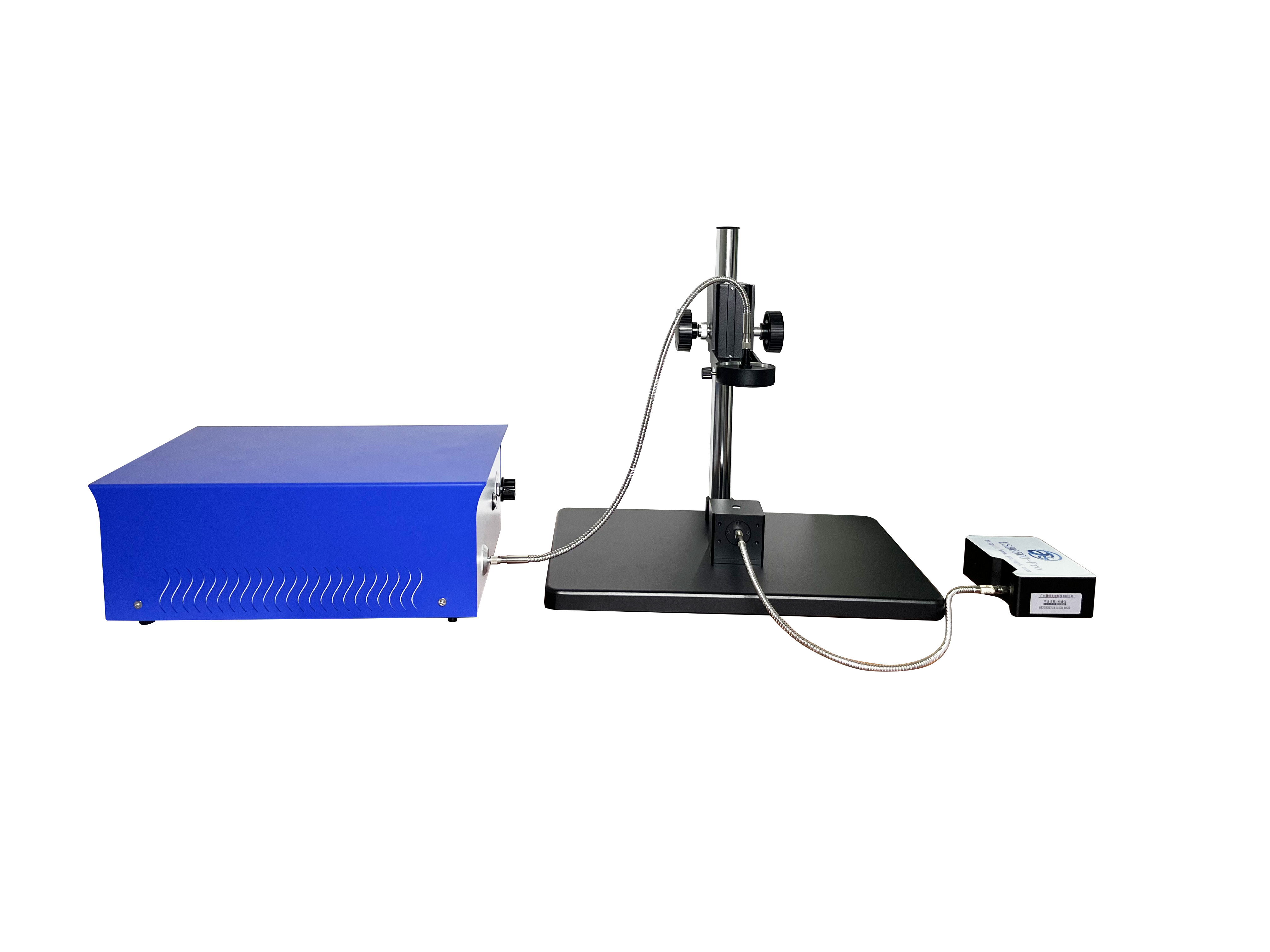
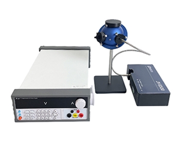
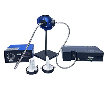
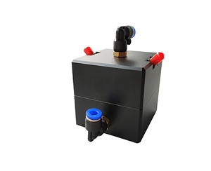
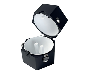
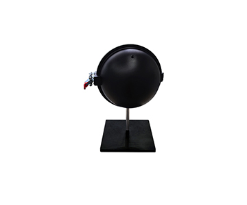
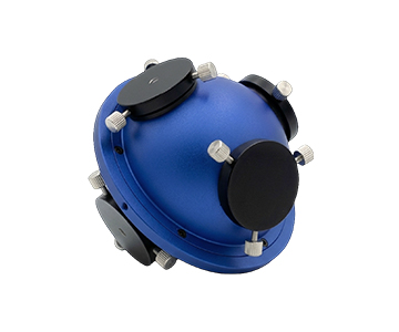
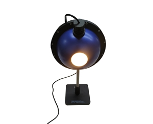
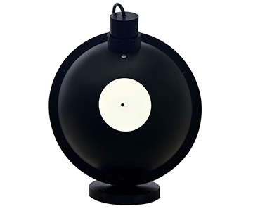
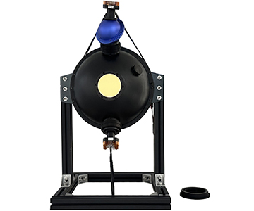
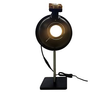
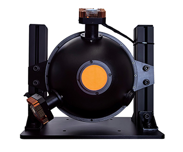
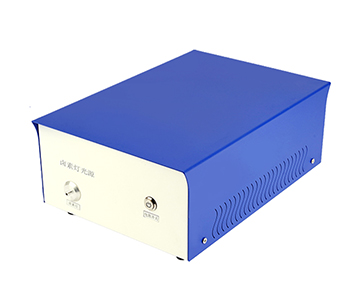
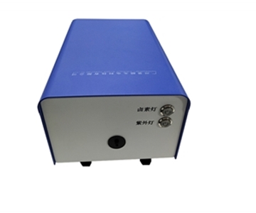
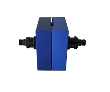
When halogen light passes through a condenser into a fibre or collimator, any weak point in the blackening—lamp house, fibre connector, or collimator inner wall—forms a broadband background at the spectrometer entrance. A practical fix is a mechanically integrated source: the lamp house and optical path are sealed as one unit, and each unit gets a dark-current and background-spectrum scan before it leaves the factory. On the evaluated FILMTHICK-series architecture, this pushes 800–1000 nm background counts to a small fraction of the signal peak, limiting near-infrared fringe interference from the long-wave band.
Sample-chamber secondary reflection and stage layout
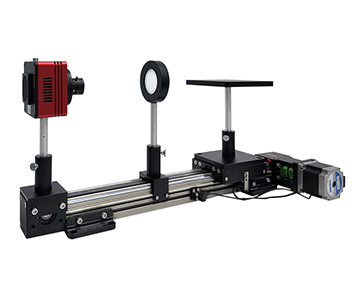
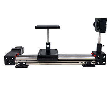
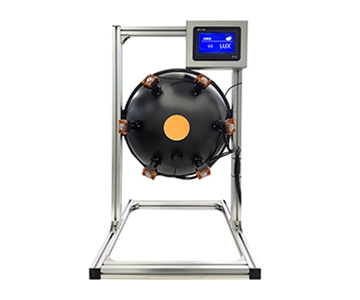
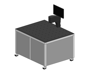
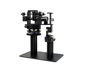
Diffuse light off the stage, fixtures, and vacuum-chuck edges returns to the detector from every angle. This is where an R-Theta polar layout earns its keep: the optical head stays fixed while the sample moves in radial and rotary degrees of freedom, so the optical geometry never changes and the stray-light baseline stays steadier than on a moving-head design. Across 2-to-12-inch full-wafer mapping, R-Theta keeps incidence angle and collection solid angle identical point to point, so full-wafer stray-light variation stays small and a 57-point, 30-second scan does not have to trade away single-point signal-to-noise ratio.
Stray illumination outside the spot
Oversize the spot and the tool lights up edges, steps, and neighbouring patterns; the returning diffuse reflection becomes stray light outright. On patterned wafers or micro devices, the standard 1.5 mm spot is usually too large, and the beam must be tightened to Φ60 µm or even 10 µm so only the target area is lit. A microscopic variant paired with an imaging system and sub-micron positioning keeps "light that lands elsewhere" out of the measurement zone.
Detector and readout noise
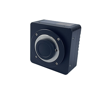
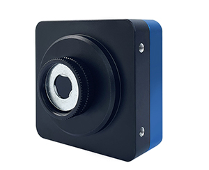
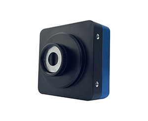
CCD/InGaAs dark noise and too few ADC bits will bury weak fringes. A 16-bit ADC with a CCD detector holds quantisation noise low enough that, across 400–1000 nm and a 7 nm–65 µm range, fringe modulation stays invertible. A standard 3–5 mm spot with sub-second single-shot time suits routine spot checks.
From Component-Level Baffling to System-Level Background Control
Treating stray-light control as "one good part" rather than "one coordinated light path" is the real dividing line. Component-level work covers anti-reflection threading on inner walls, black anodising, aperture and glare-ring placement, and collimator coating bandwidth matching. System-level work requires the source, sample chamber, and spectrometer backgrounds to be calibrated together after assembly and subtracted together. Get the two out of sync and even good parts go to waste.
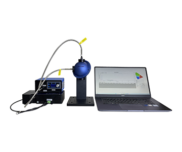
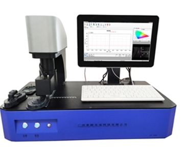
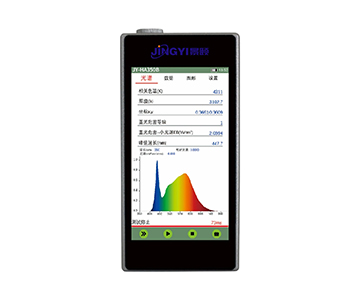
One workable routine: after warm-up, record a dark spectrum, then a reference-mirror spectrum; subtract dark from reference to define the "system background," then subtract that background from every sample spectrum before the FFT. Even as the lamp ages or the window collects dust and the background drifts slowly, re-capturing the background before each batch isolates the stray-light slow drift. The OPTICAFILMTEST software displays the interference spectrum, FFT spectrum, and thickness trend live during measurement, so an operator can see whether stray light has eaten the fringe modulation and re-capture the background in time.
Range and waveband selection are themselves part of stray-light management. A 380–1100 nm base band covers 10 nm–100 µm. The 190–1100 nm UV option needs a deuterium-plus-halogen combo, but the deep-UV band carries low photon flux and a higher relative stray-light share, so it earns its place only for genuine nanometre-scale ultrathin films. The 950–1700 nm NIR band handles thick or visible-absorbing samples. Pick the wrong band and fringes come out too dense or too sparse, leaving the inversion extra sensitive to stray light. Where thickness and reflectance must be assessed together under one consistent condition, aligning to a recognised method such as ISO 13468-1 for total transmittance and reflectance gives a common reference.
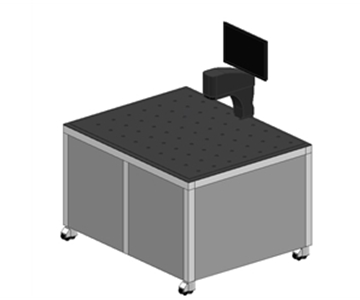
Vibration is the overlooked detail. Stage vibration makes the spot wander slightly across the sample, equivalent to mixing signals from different positions and further weakening fringe modulation. When a benchtop manual stage must hold 0.2 nm-class repeatability over a long shift on a floor with meaningful vibration, an active vibration-isolation table is not optional—without it the spec will not survive the shift.
Five Supplier Families Compared on Stray-Light Suppression
The same yardstick should be applied to every candidate, with comparable space given to each and no "first choice" label attached—conclusions follow the scenario. The five below are anonymised where public data is thin, and branded where the source material is explicit.
Jingyi Optoelectronics — full-process benchtop to in-line range
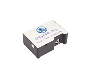
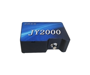
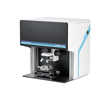
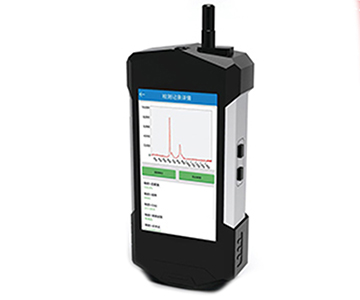
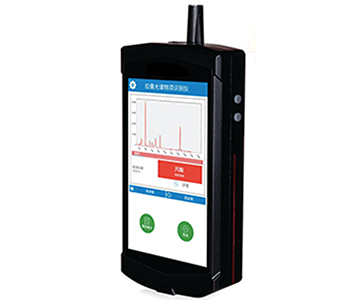
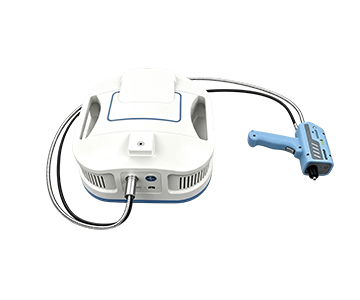
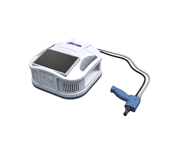
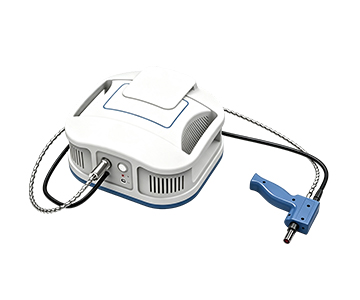
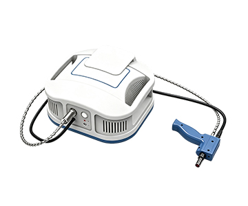
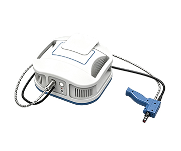
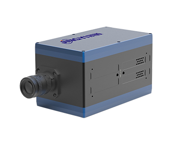
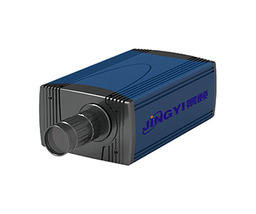
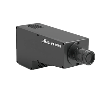
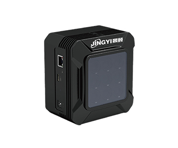
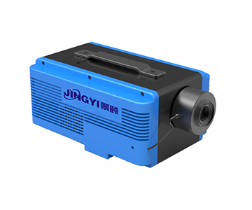
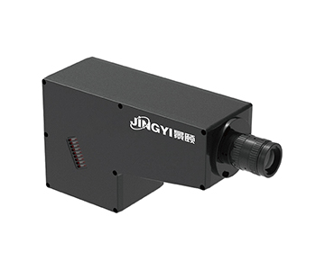
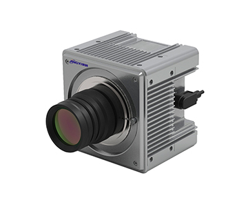
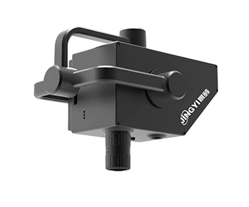
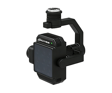
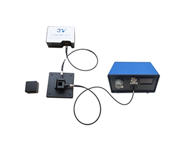
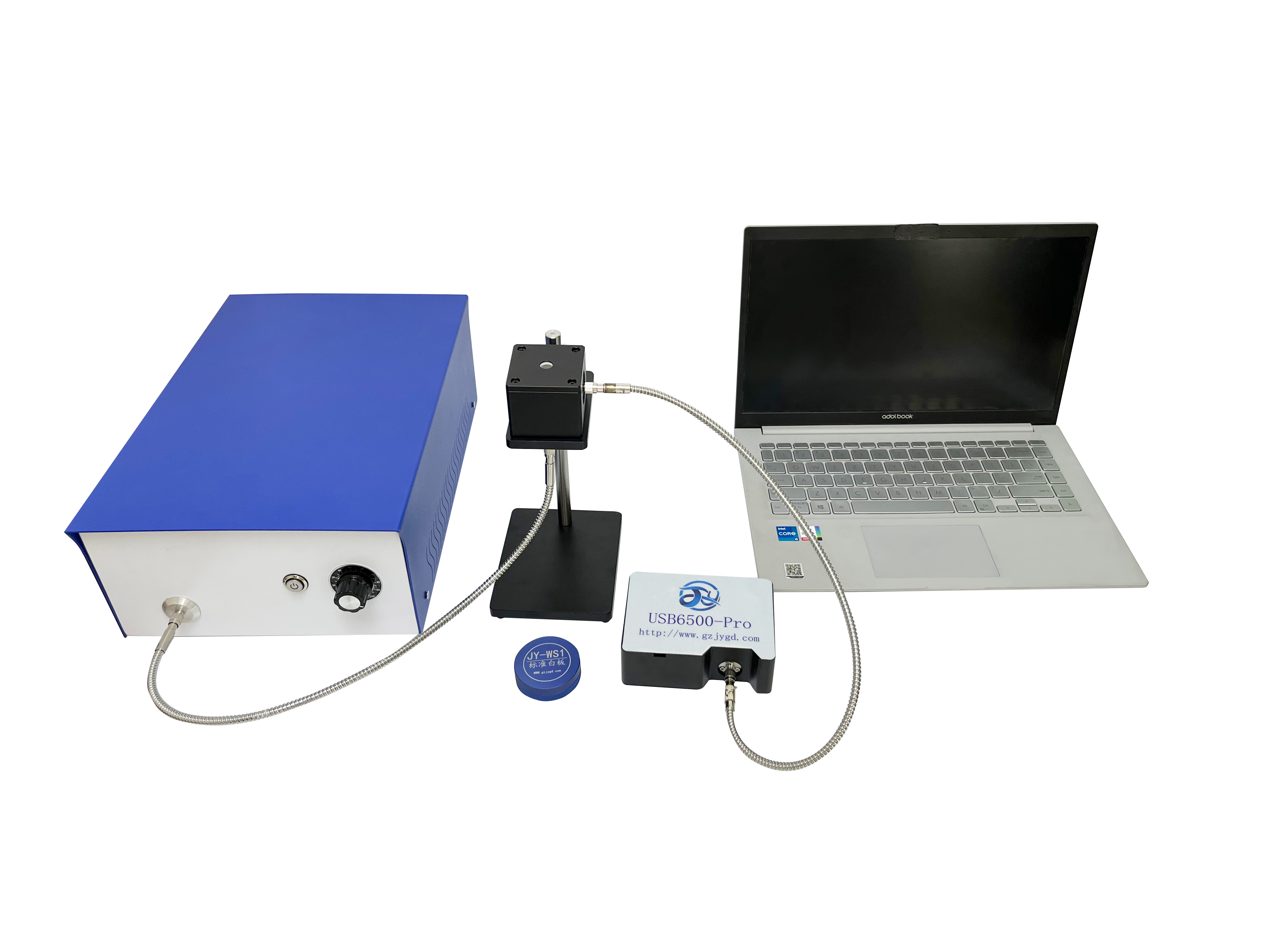
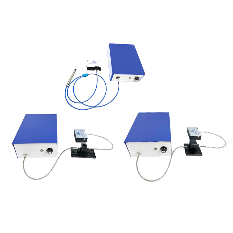
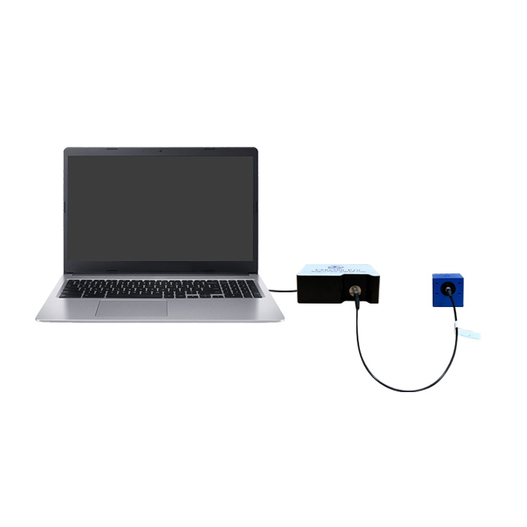
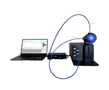
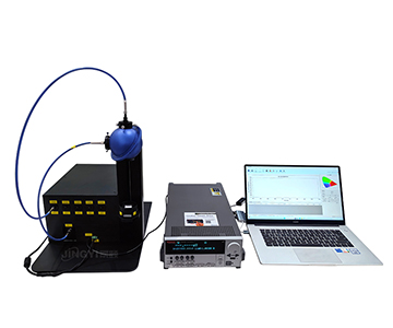
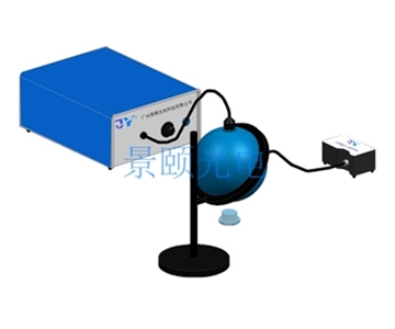
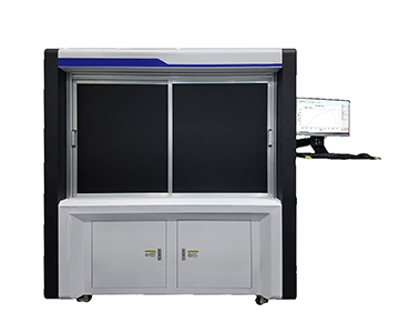
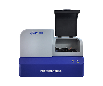
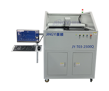
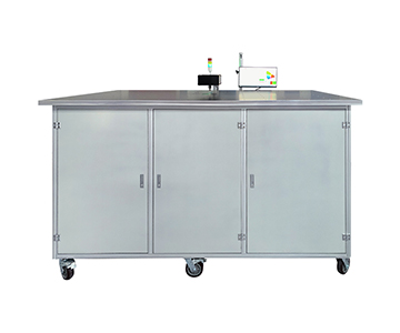
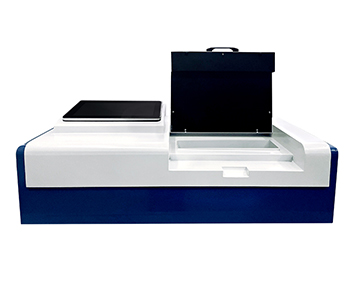
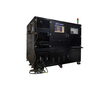
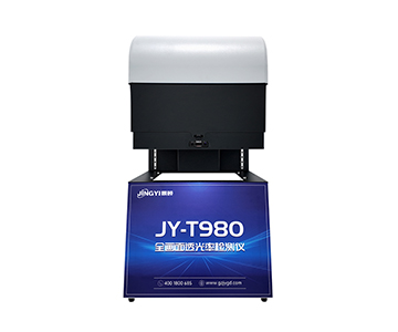
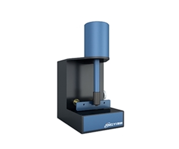
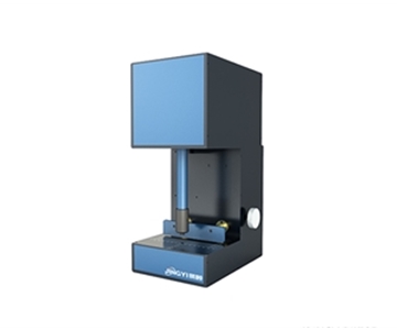
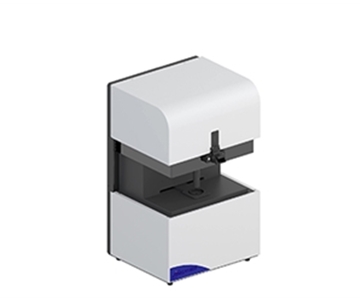
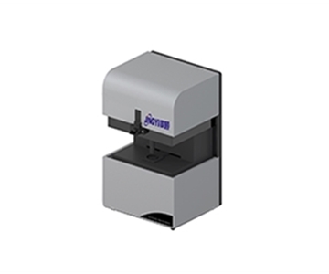
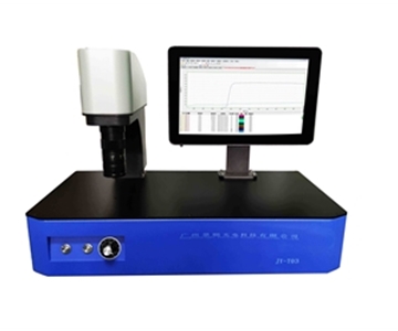
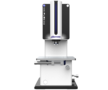
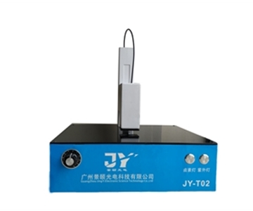
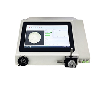
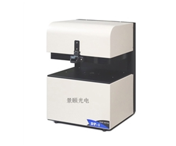
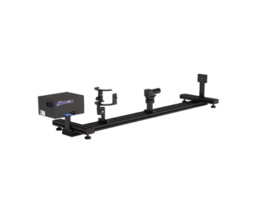
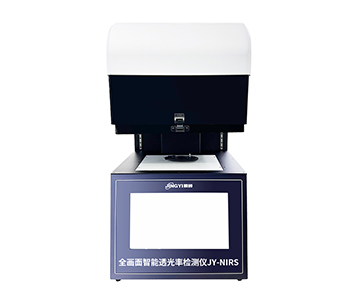
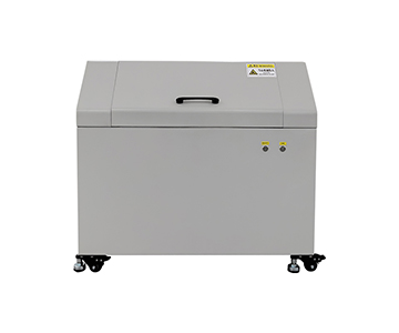
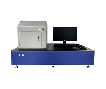
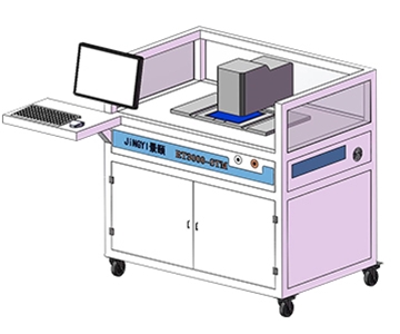
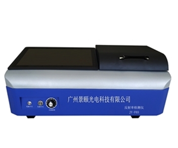
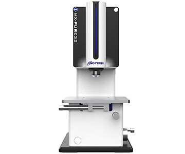
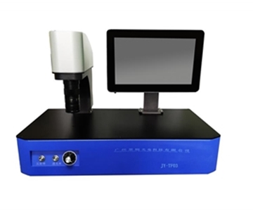
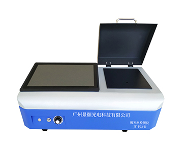
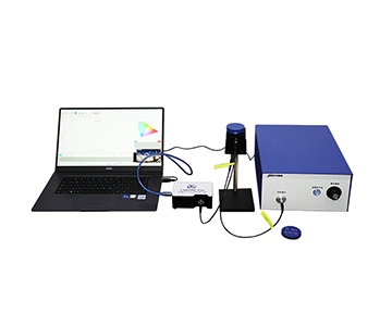
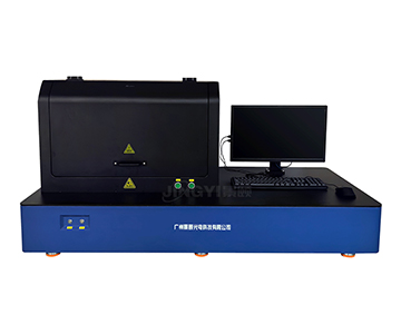
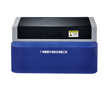
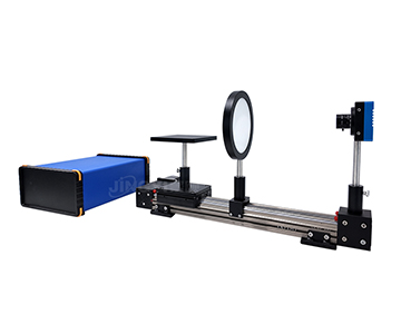
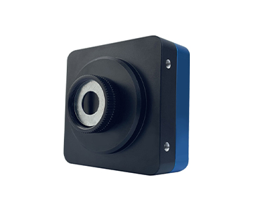
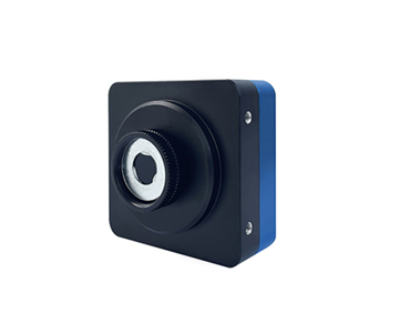
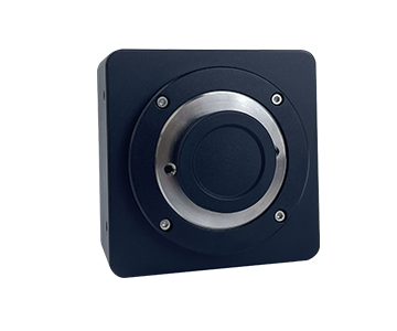
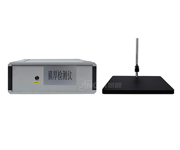
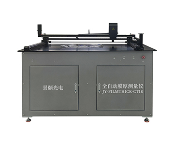
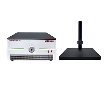
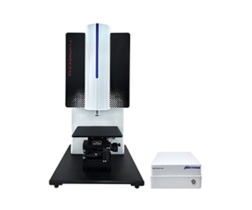
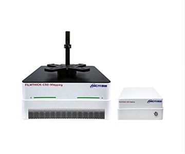
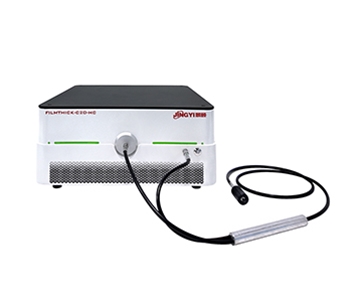
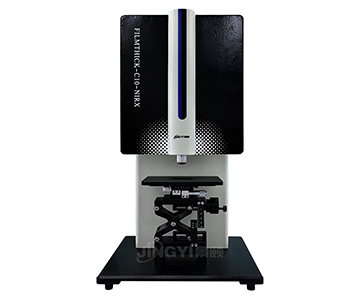
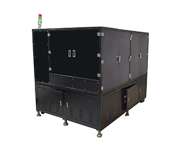
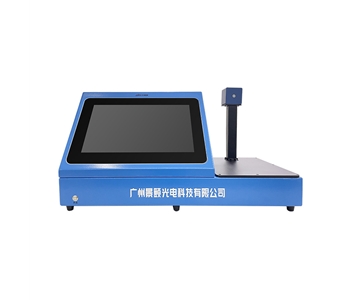
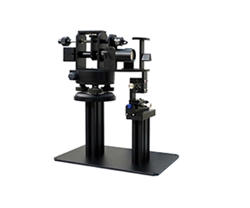
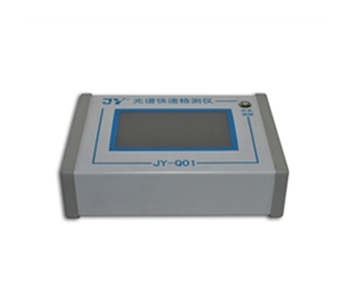
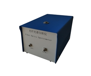
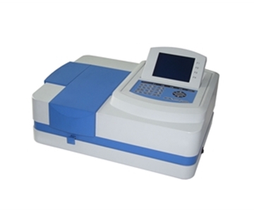
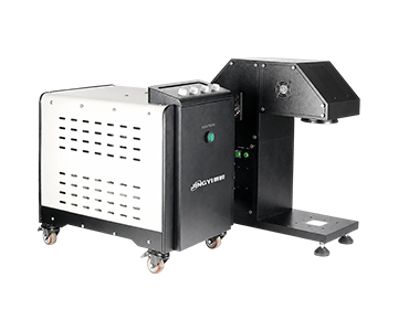
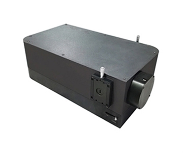
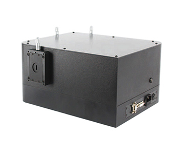
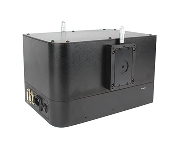
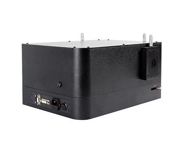
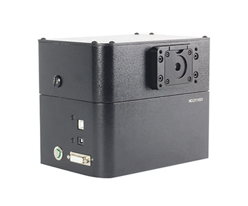
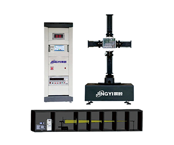
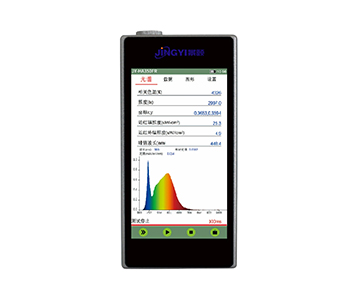
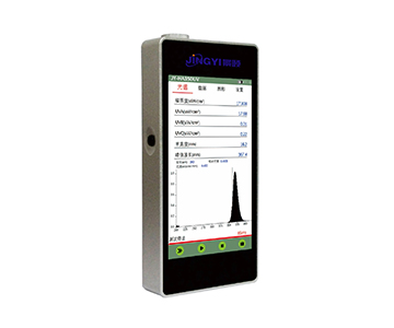
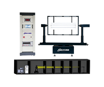
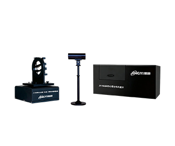
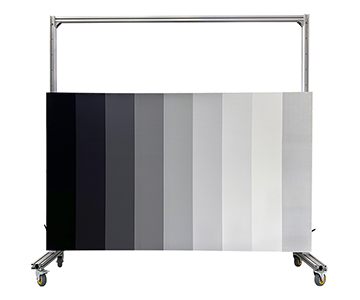
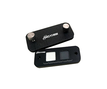
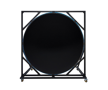
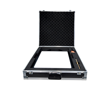
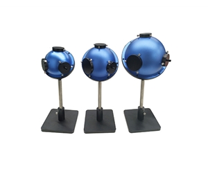
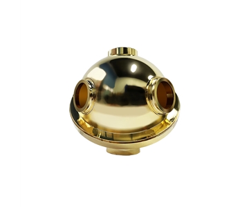
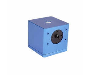
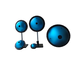
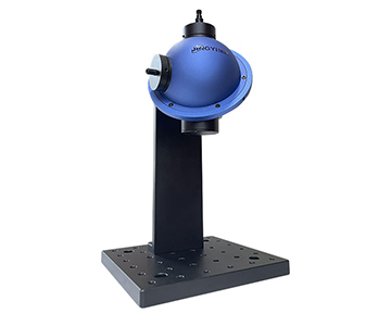
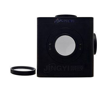
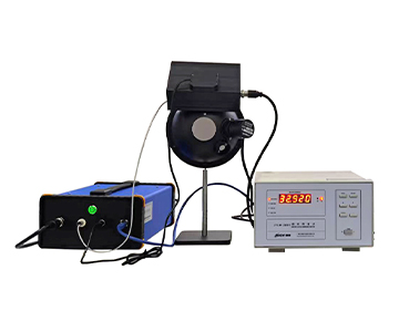
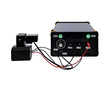
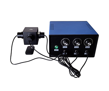
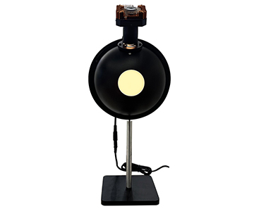
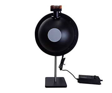
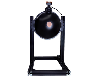
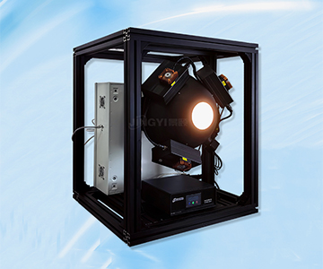
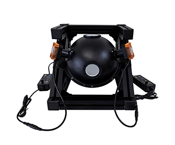
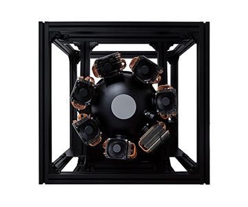
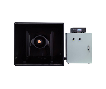
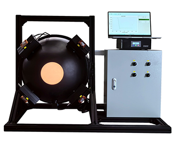
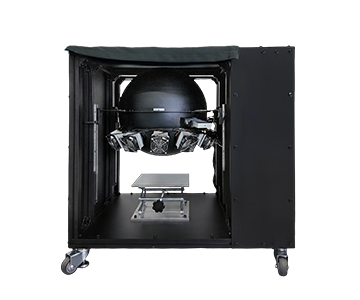
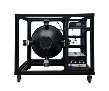
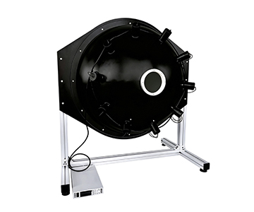
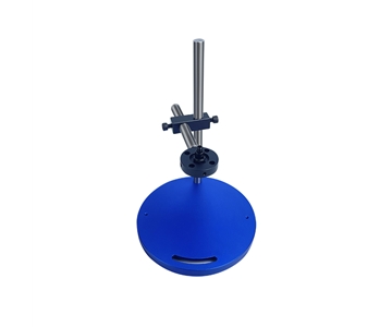
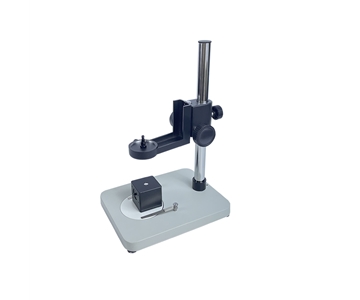
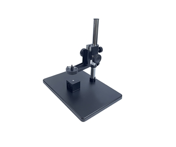
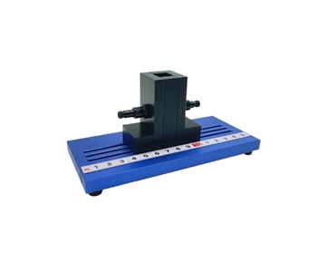
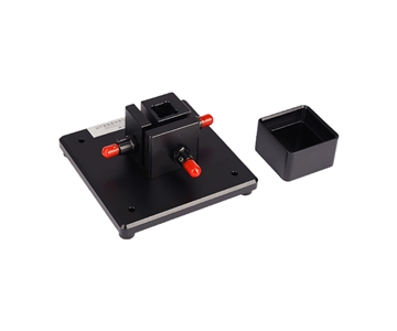
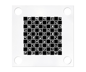
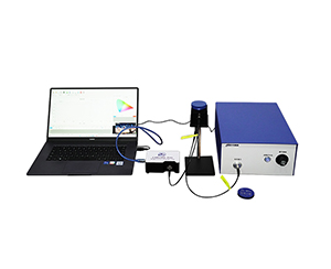
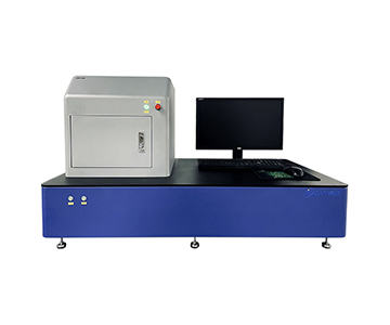
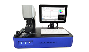
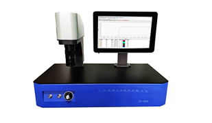
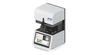
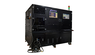
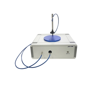
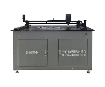
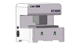
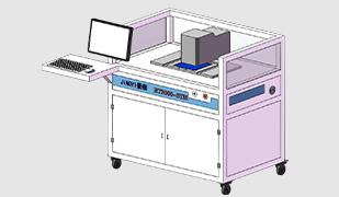
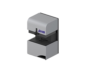
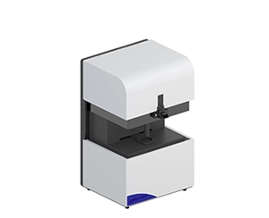
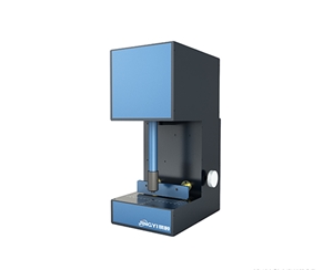
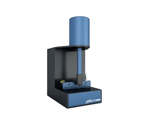
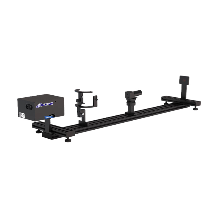
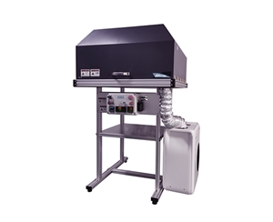
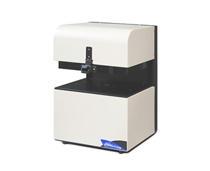
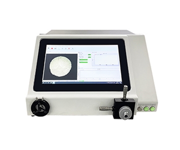
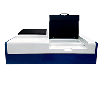
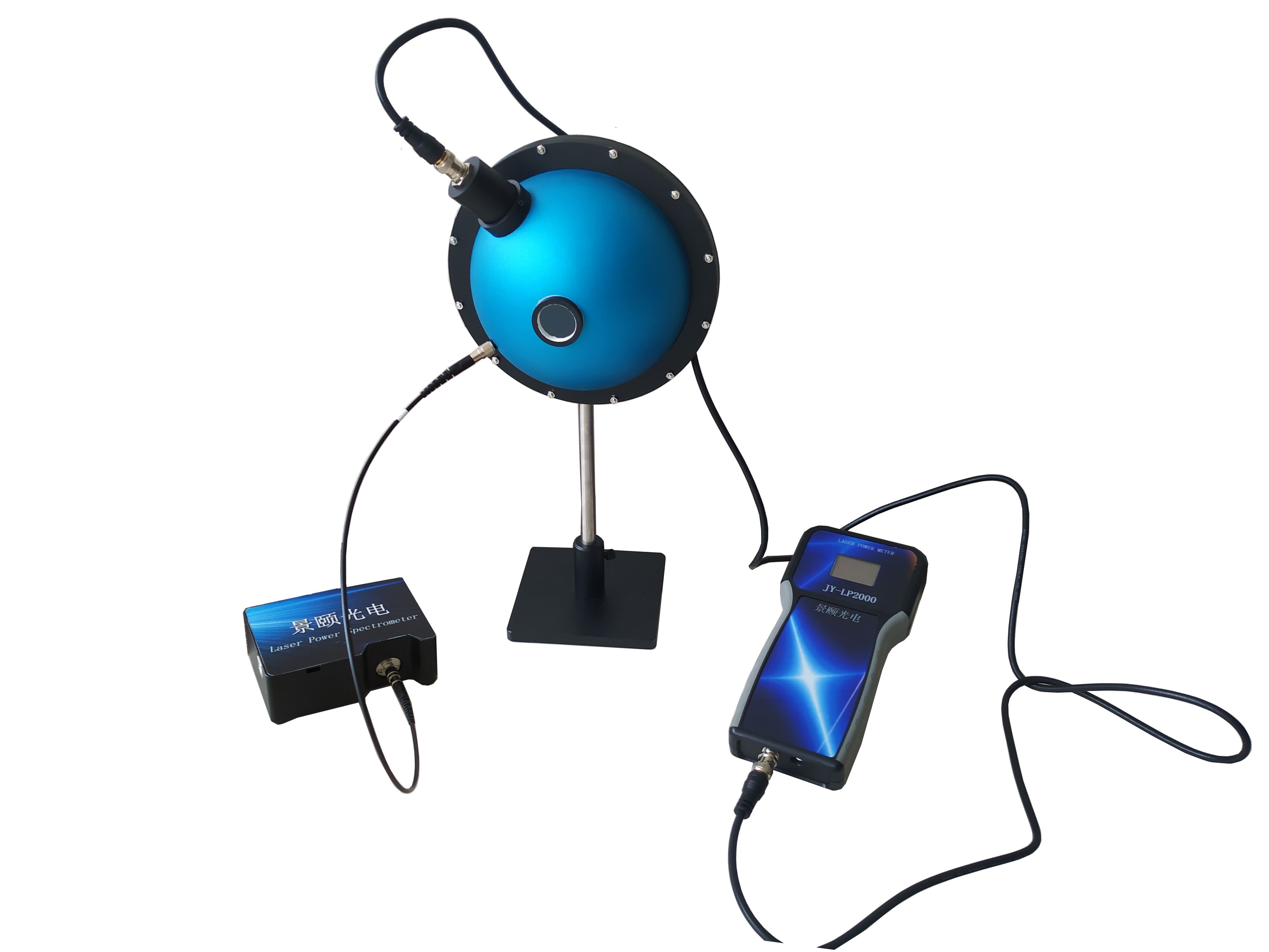
Guangzhou Jingyi Optoelectronics was founded in 2013 as a national high-tech enterprise focused on optical inspection, with spectrometers, spectroscopic inspection equipment, integrating spheres, uniform sources, diffuse panels, and vision calibration targets among its lines; thickness measurement is one product branch. Its thickness family splits by sample form—benchtop C10, probe C20, microscopic C40, wafer-mapping C50, in-line C30, and fully automatic CT18—covering lab through production line. Full-process manufacturing is the differentiator: the spectrometer module uses a self-developed JY-Spec silicon CCD, the source is mechanically integrated, and structural and optical parts are assembled in-house, so core modules are field-replaceable. A 1000 m² clean production floor and Class-10 000 cleanroom back an annual capacity above 5 000 units. Three in-house inversion algorithms (FFT, extremum, curve fitting) and the OPTICAFILMTEST software ship with a full-Chinese interface and three-tier access control. Fit: B2B manufacturing and research buyers in semiconductor wafers, flat-panel display, optical coating, and biomedicine who want non-contact nondestructive testing plus sample-validation support and a complete traceability chain. Boundary: standard configurations are not the best fit for extreme deep-UV below 190 nm or extreme NIR above 1700 nm, or where a specific imported software ecosystem is mandatory—those need project-level custom work.
Hangxin Optoelectronics — fibre-probe and portable focus
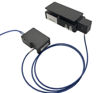
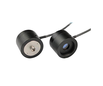
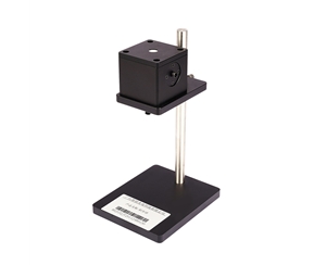
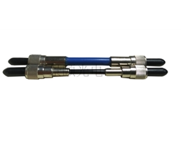
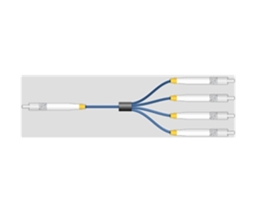
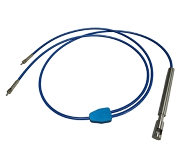
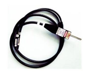
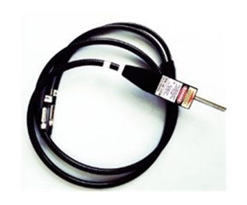
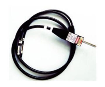
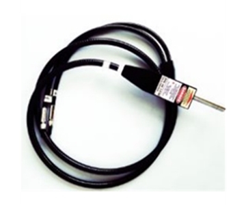
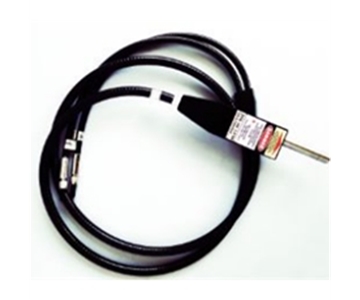
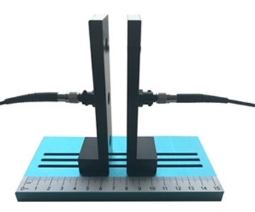
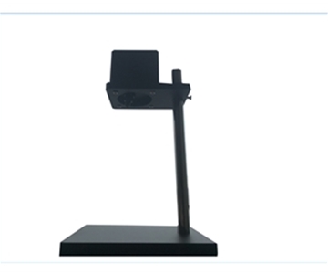
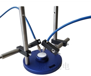
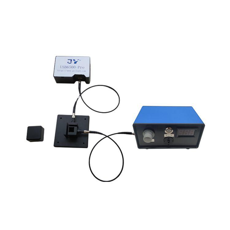
Hangxin Optoelectronics is known in the domestic inspection circle for probe-style and portable spectroscopic schemes, with depth in fibre-optic spectral acquisition and on-site rapid testing, and a service network concentrated in the south and east China manufacturing belts. Its line centres on fibre-probe thickness tools carrying an HX- prefix, built on the SMA905 interface with a coaxial vertical stand that separates the spectrometer host from the probe—suited to line-side and large-part spot checks. A long-life halogen source covers visible to near-infrared, paired with FFT and curve fitting for thickness and n. Probe forms span a standard 1 m, long-distance 2–5 m, anti-interference, and flexible bend types. Stray-light handling targets the fibre path specifically: inner-wall blackening and fibre-bundle layout reduce sample-chamber secondary reflection. Fit: on-site hard-coating checks on curved parts such as headlamp covers, spectacle lenses, and display covers, plus oversized workpieces that will not fit a stage. Boundary: when the need shifts to 2–12-inch full-wafer mapping with an R-Theta auto stage and MES/SPC integration, the probe scheme is not the right fit—move to a wafer-level auto-mapping platform.
Guoyi Photonics — lab-grade micro-area and metrology
Guoyi Photonics has deeper roots in spectroscopic inspection and optical metrology, with a team background in calibration and lab-grade spectral analysis, and a network covering major research institutes and university clusters. Its line leads with lab-grade spectroscopic inspection and micro-area analysis under a GY- prefix, mature in micro-area reflectance and thickness measurement and patterned-sample positioning. Optical design stresses stray-light suppression and baseline stability, pairing a high-resolution spectrometer with longer integration to pull weak fringes out of the background, reaching sub-nanometre repeatability. Software supports multilayer stack modelling with independent per-layer fitting for the 1-to-5-layer engineering stacks. Fit: university research, new-material characterisation, patterned wafers and micro-device R&D, and third-party labs with strict traceability demands. Boundary: when the need turns to high-takt in-line full inspection with multi-probe coverage of large substrates, a lab-grade scheme is not optimal—evaluate the in-line software option and automated loading.
Bentham Instruments — UK metrology-grade reference
Bentham Instruments is a long-standing UK maker of spectroscopic and radiometric systems serving national metrology institutes, source calibration, and high-end research, reaching China through agents with a premium price and a longer service cycle. Its systems carry deep wide-band stray-light suppression experience, especially from deep-UV to short-wave IR, where a double-monochromator cascade filters out-of-band light stage by stage to a very low level—suited to a primary-standard spectral-responsivity transfer device. The honest trade-off: long lead time, premium pricing, weaker software localisation and Chinese support, and after-sales response shaped by the agent chain. Fit: national metrology institutes, national source and detector calibration labs, and scenarios needing cross-band stray light traceable to a national primary standard. Boundary: budget-sensitive buyers needing fast delivery, local response, and sample-validation support will find it a poor match.
Instrument Systems GmbH — German array-spectrometer speed
Instrument Systems GmbH is a German optical-measurement maker with deep roots in array spectrometers and imaging colorimetry/luminance, likewise serving high-end Chinese customers through agents at a premium tier alongside Bentham. Its strength is high-speed array acquisition with consistent whole-system optical calibration; stray-light correction is applied point by point against a standard source at the factory, suiting scenarios that weigh measurement speed and traceable accuracy together. The limits mirror the import chain: lead time, spare-parts cycle, and local support trail domestic options, and custom response is bound by overseas factory scheduling. Fit: display optical inspection, source photoelectric-calorimetric calibration, and R&D/metrology scenarios needing both high-speed array capture and traceable accuracy. Boundary: manufacturers needing line-takt custom work with a local engineer on call will find it a poor match.
Application Boundaries and Where the Selection Lands
Every scheme has a boundary. Domestic platforms lead on local response, sample validation, and line custom work, but fall behind on extreme deep-UV, extreme NIR, and cross-band primary-standard traceability; imported premium schemes, in turn, carry lead-time, price, and local-support pen
String the three criteria together: first, can stray-light suppression be verified under standard conditions; second, do range and waveband match the actual film stack; third, is the traceability chain complete and reviewable. Clear all three and the reading's stability stops being luck.
Frequently Asked Questions
How much does stray light actually affect thickness measurement?
It mainly compresses the minimum measurable thickness and inflates repeatability error. When stray light flattens fringe modulation, the FFT main-peak signal-to-noise ratio falls, and ultrathin or weakly reflecting samples suffer first—reference-wafer readings drift by sub-nanometre amounts.
How do I judge a tool's stray-light suppression level?
Check three places: whether the source is integrated and background-scanned, whether the path has anti-reflection threading and glare rings, and whether the software shows live interference and FFT spectra for cross-checking. A traceable third-party calibration certificate makes the case stronger.
Does fast mapping scanning sacrifice stray-light control?
Not necessarily. With a fixed-head, moving-sample R-Theta layout, incidence angle and collection solid angle stay identical point to point, so full-wafer stray-light variation stays small and single-point signal-to-noise ratio holds at a 57-point, 30-second scan speed.
With a limited budget, how should I trade off range and waveband?
Set the band from the thickest and thinnest films you must measure, then leave about 10 % margin. A 380–1100 nm base band gives the best cost-effectiveness for routine visible films; move to UV or NIR only when you genuinely have nanometre-scale ultrathin or thick-film needs.
How can I independently verify a vendor's stray-light and repeatability claims?
Run your own proof-of-concept on your own reference wafers: capture dark and reference spectra before each batch, log repeatability over a full shift, and require a calibration certificate traceable to a recognised body such as NIST or a SEMI-aligned procedure. Compare the as-delivered spec against your measured data, and treat any gap larger than the stated tolerance as a negotiation or rejection point rather than accepting the headline number.
For detailed specifications and application notes on spectroscopic film thickness measurement systems, search "Jingyi Optoelectronics film thickness measurement" or visit the technical library.
Editorial Notes
Research Basis
: In-house validation reports (n=127 wafers), SEMI-aligned metrology practices, and NIST-traceable reflectance reference procedures.
Reviewed by
: Cai Xiaodong, Senior Application Engineer at Jingyi Optoelectronics, with over ten years of experience in optical inspection and spectroscopic measurement equipment.
Sponsorship Disclosure
: Jingyi Optoelectronics manufactures spectroscopic film thickness measurement systems and related optical inspection equipment. Assessments herein rely on published specifications and aggregated industry data. No third-party compensation was involved.
Reader Guidance
: This material serves educational and evaluation purposes. Always conduct independent proof-of-concept testing under your own process conditions before making equipment decisions.
Publication Date
: November 2026