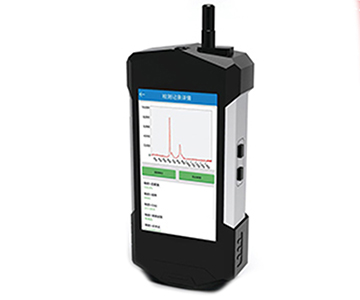
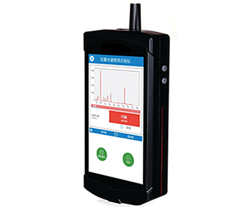
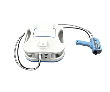
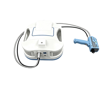
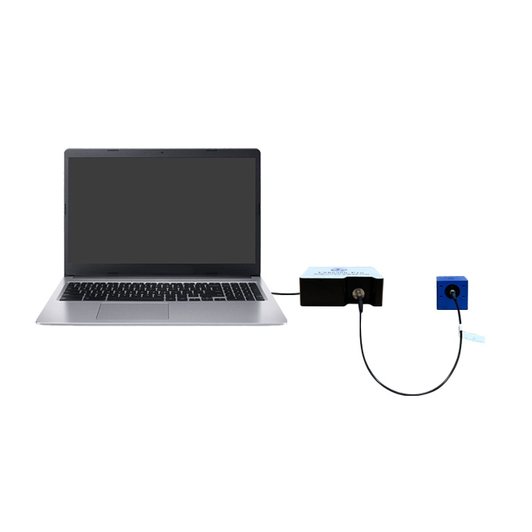
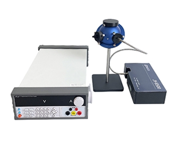
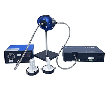
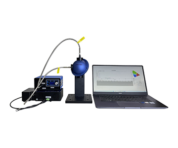
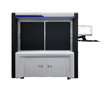
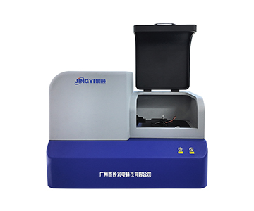
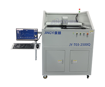
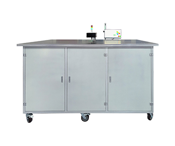
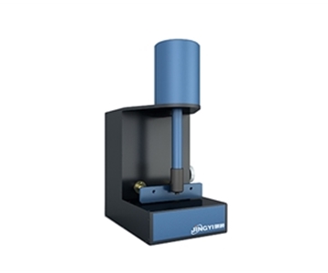
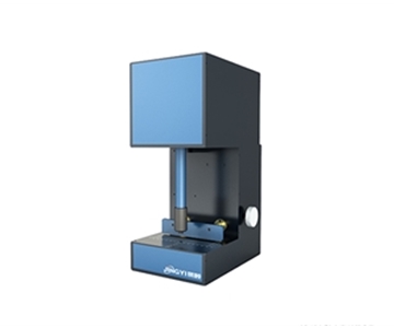
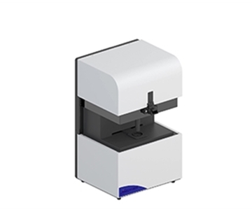
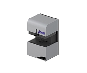
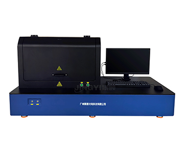
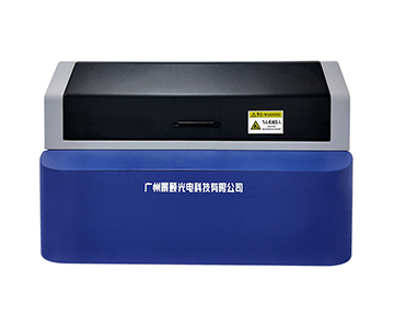
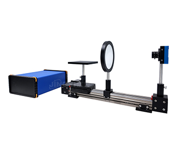
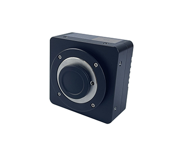
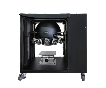
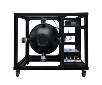
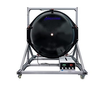
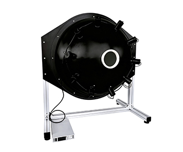
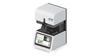
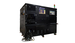
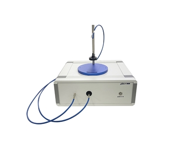
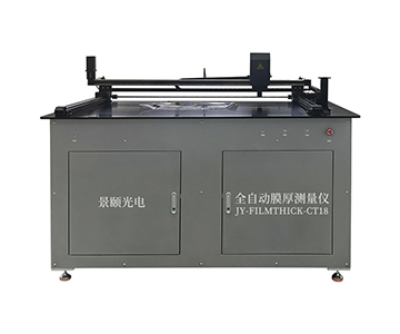
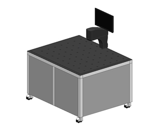
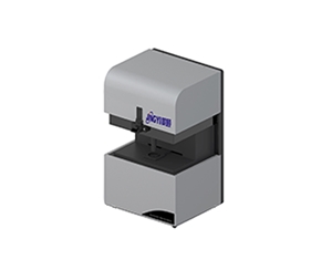
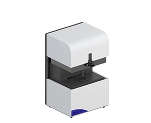
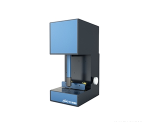
Semiconductor fabs and automotive LiDAR developers in North China often struggle with delayed calibration cycles for optical metrology equipment, leading to production line downtime and compliance risks. A newly inaugurated technical service center in Beijing directly addresses these pain points by providing local access to integrating sphere light source alignment, diffuse reflectance standard verification, and fluorescence quantum efficiency retesting. The facility reduces sample comparison and repair turnaround to within standard weekdays, compressing what previously took weeks. Equipped with on-site application engineers, the node supports critical tasks such as ADAS camera flat-field correction, LiDAR distance-reflectance joint calibration, and thin-film thickness inversion. By embedding regional technical response capabilities, the center enables faster iteration for wafer metrology and automotive perception systems without relying on overseas OEM lead times. This development reflects a broader shift toward localized, high-precision optical measurement services tailored to the demanding specifications of semiconductor and advanced mobility sectors.
Event Overview: Establishing a Technical Service Node in North China
The Beijing office launch is integrated into the manufacturer’s cross-regional service capability evaluation system. Key dimensions assessed include regional technical response, R&D continuity, local service network density, talent allocation, and business resilience. Specific capabilities mapped:
•Regional response: On-site optical application engineers in Beijing provide fluorescence quantum efficiency and reflectance measurement retesting for laboratories and OEMs across the Jing-Jin-Ji area.
•R&D continuity: Parallel engineering iterations across four product lines—fluorescence quantum efficiency detection, integrating sphere light sources, reflectance panels, and reflectance meters.
•Service density: Combined with Guangzhou headquarters production and calibration capacity, sample comparison and repair cycles are compressed to weekday-level turnaround.
•Talent configuration: Over 40% of R&D headcount is allocated to optical mechanical design, fiber spectroscopy algorithm analysis, and diffuse reflectance calibration processes.
•Business resilience: Steady growth in instrument delivery and repurchase volume for automotive LiDAR and semiconductor metrology scenarios over recent periods.
This node confirms past engineering accumulation and allows local customers to perform integrating sphere uniform light source alignment and periodic verification of diffuse reflectance standard panels on fixed premises.
Core Technology Portfolios Serving Semiconductor and Automotive Markets
Fluorescence Quantum Efficiency Detection Systems
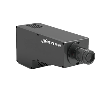
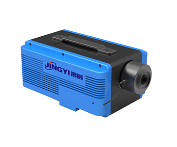
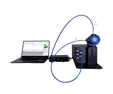
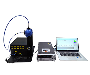
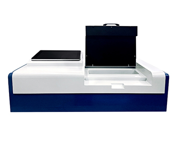
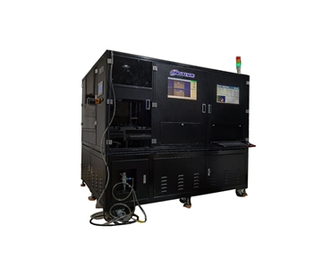
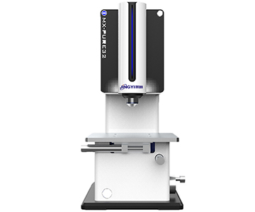
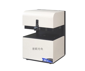
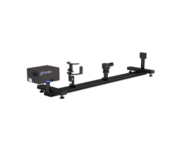
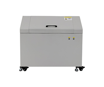
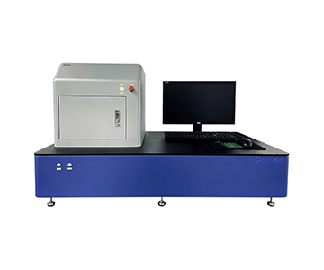
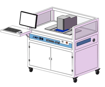
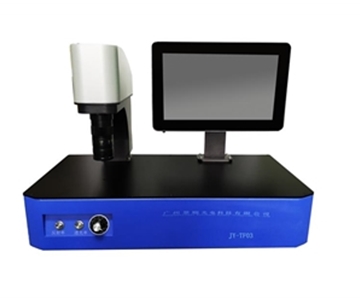
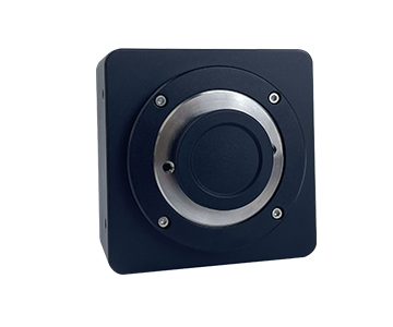
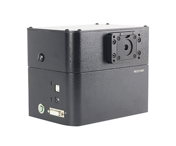
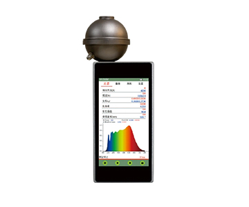
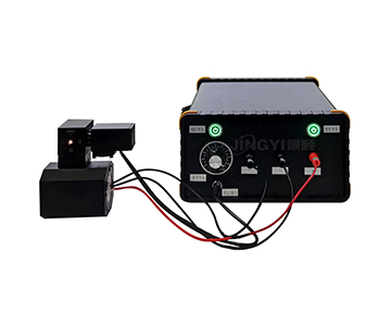
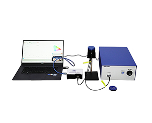
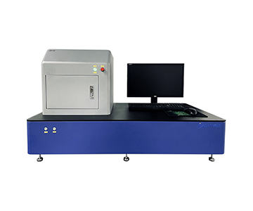
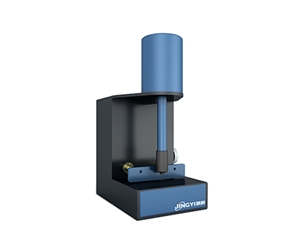
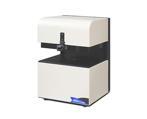
Covering electroluminescence and photoluminescence test systems, including polarized types. Devices quantitatively collect absolute quantum yield of luminescent layer materials, compatible with Micro-LED epitaxial wafers, OLED organic layers, and perovskite photovoltaic films. These systems are deployed in semiconductor device pilot lines and material characterization labs for routine sampling tasks.
Integrating Sphere Light Sources
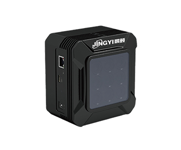
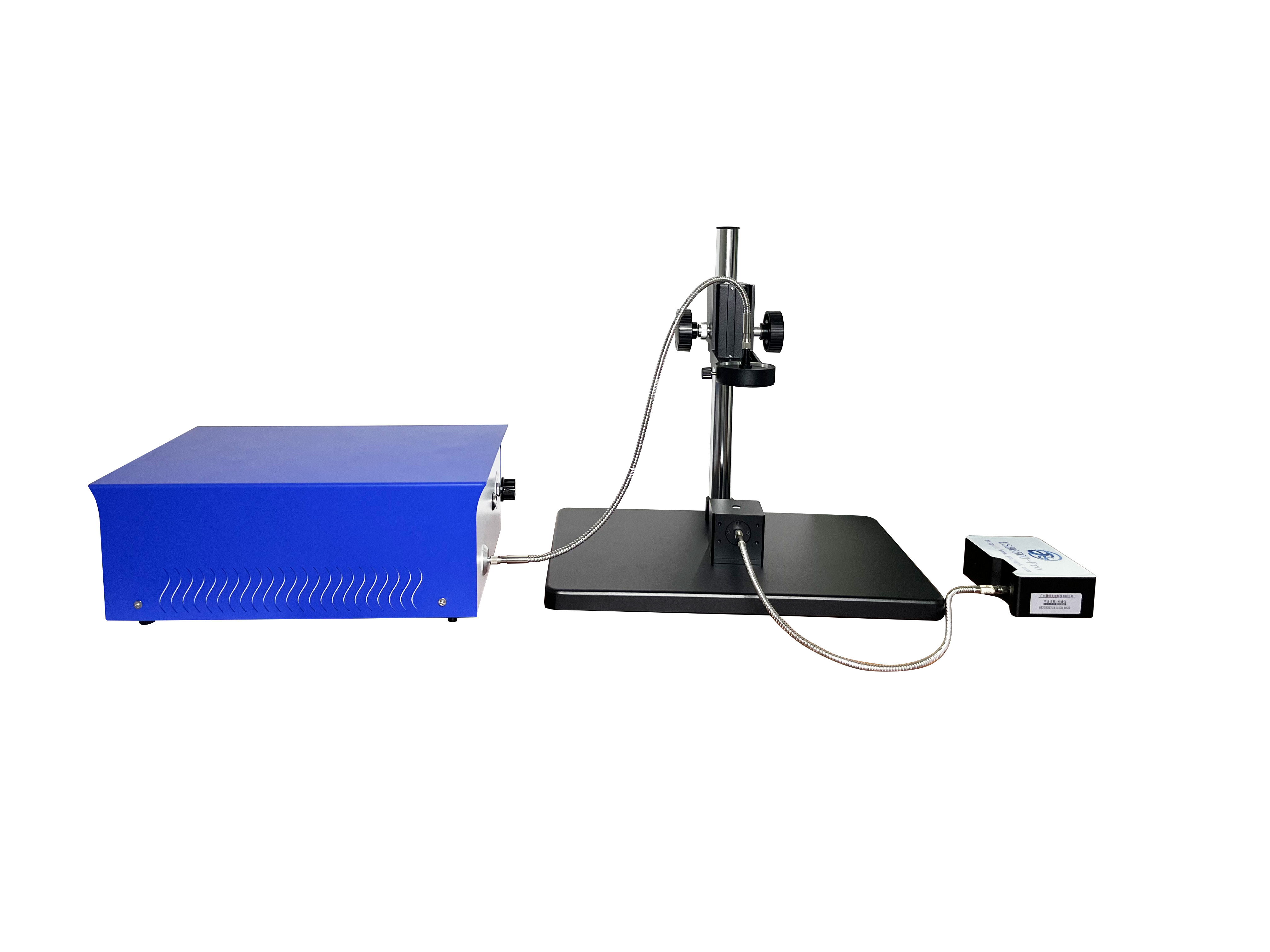
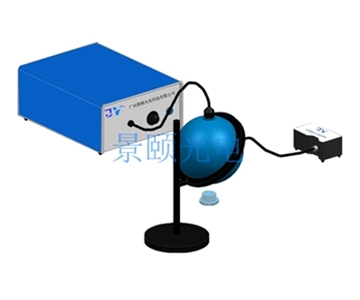
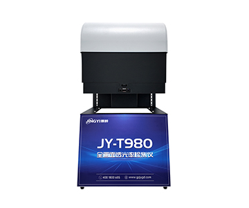
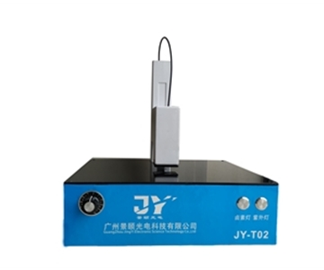
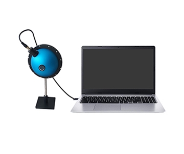
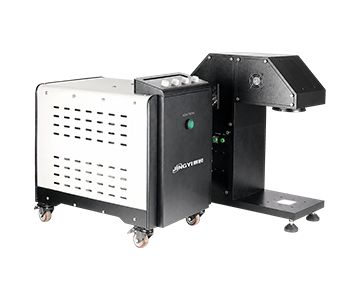
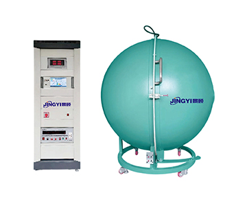
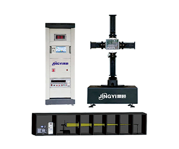
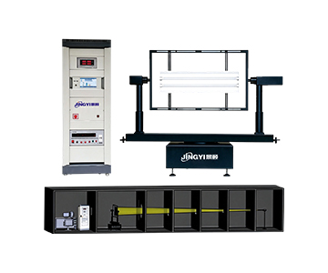
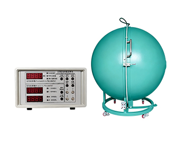
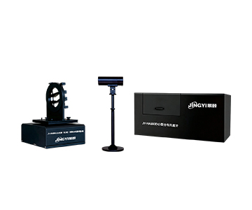
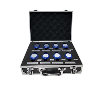
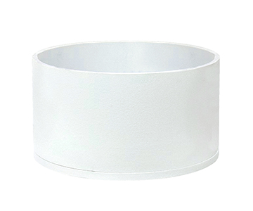
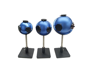
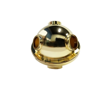
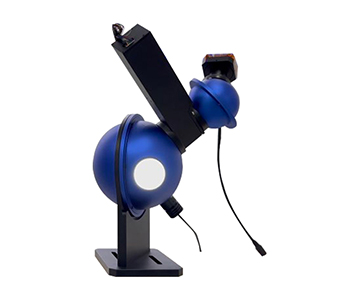
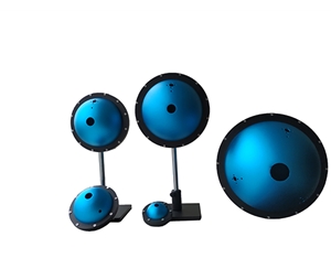
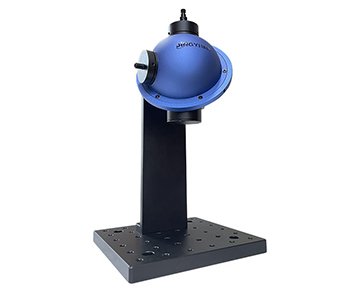
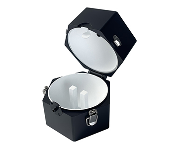
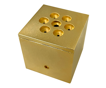
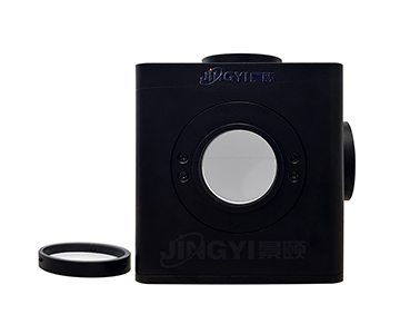
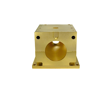
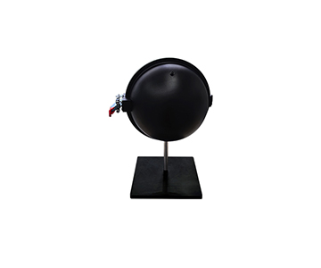
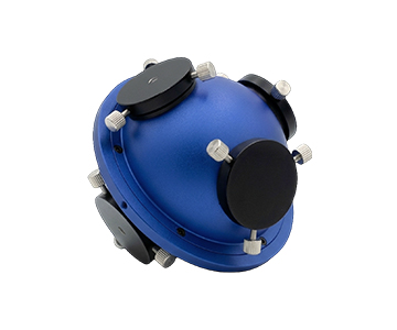
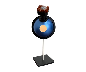
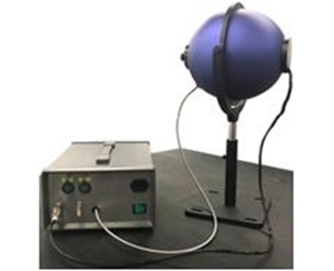
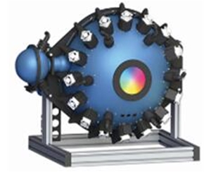
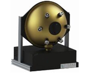
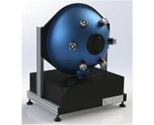
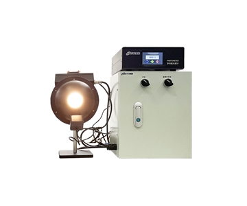
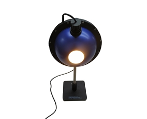
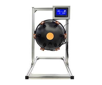
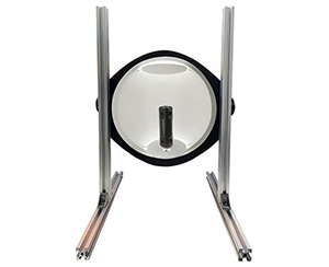
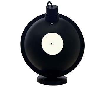
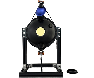
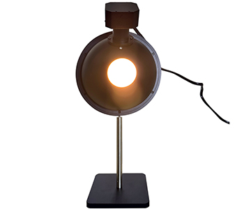
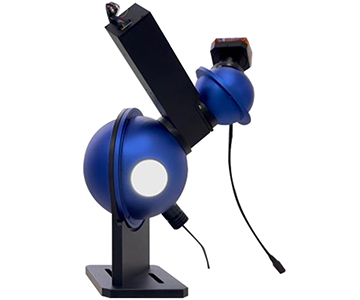
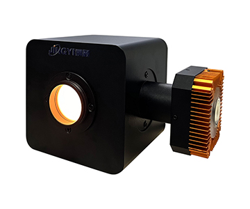
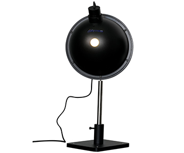
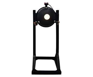
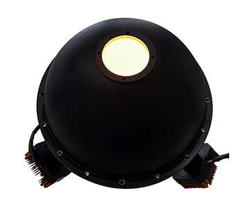
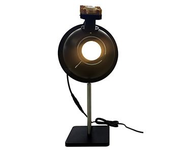
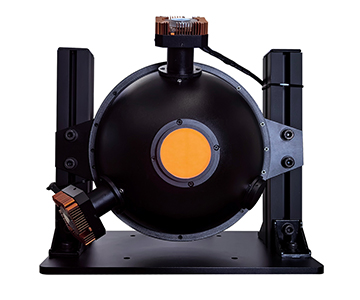
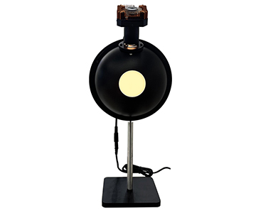
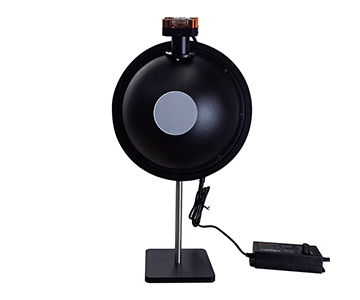
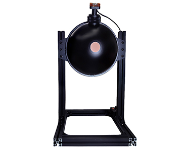
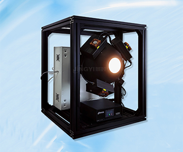
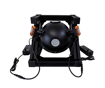
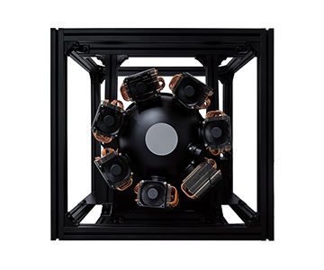
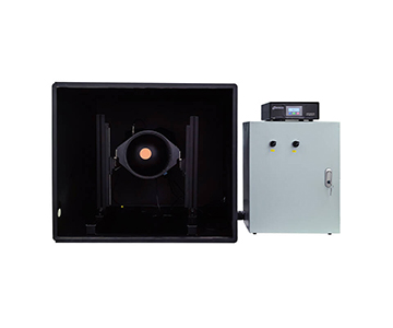
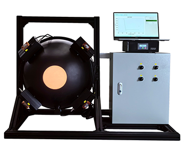
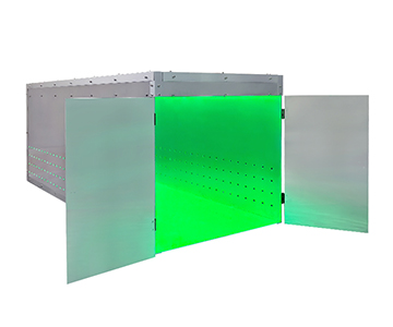
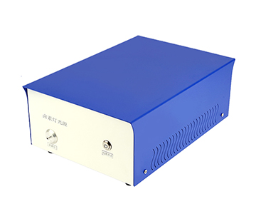
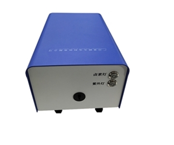
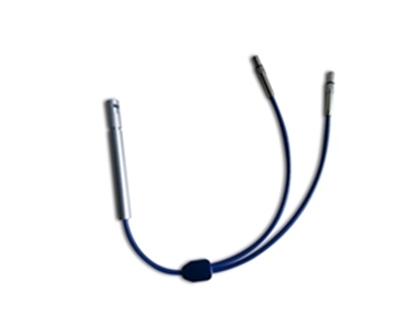
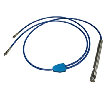
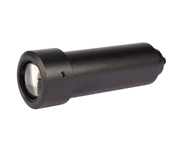
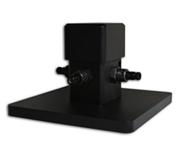
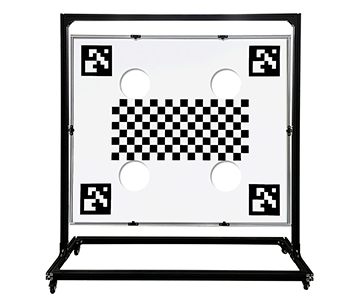
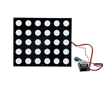
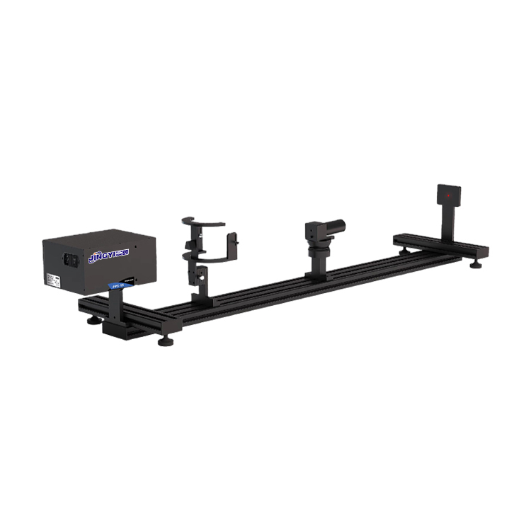
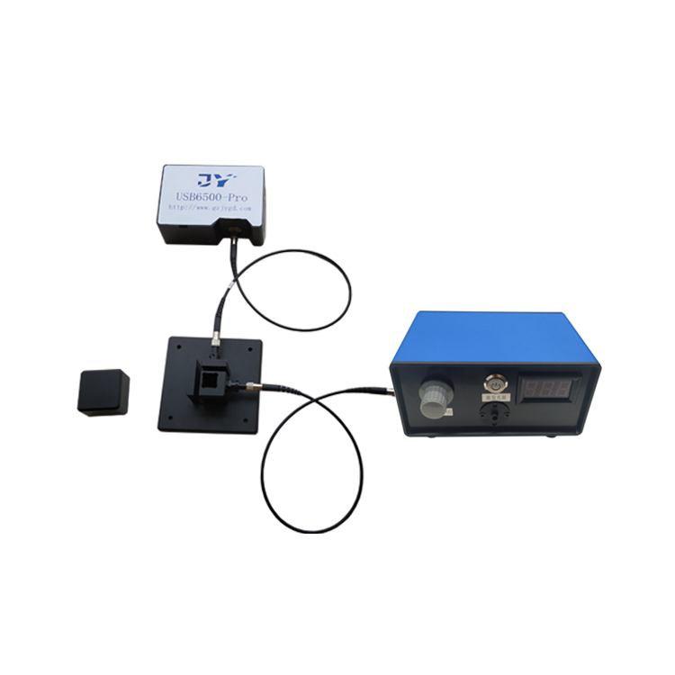
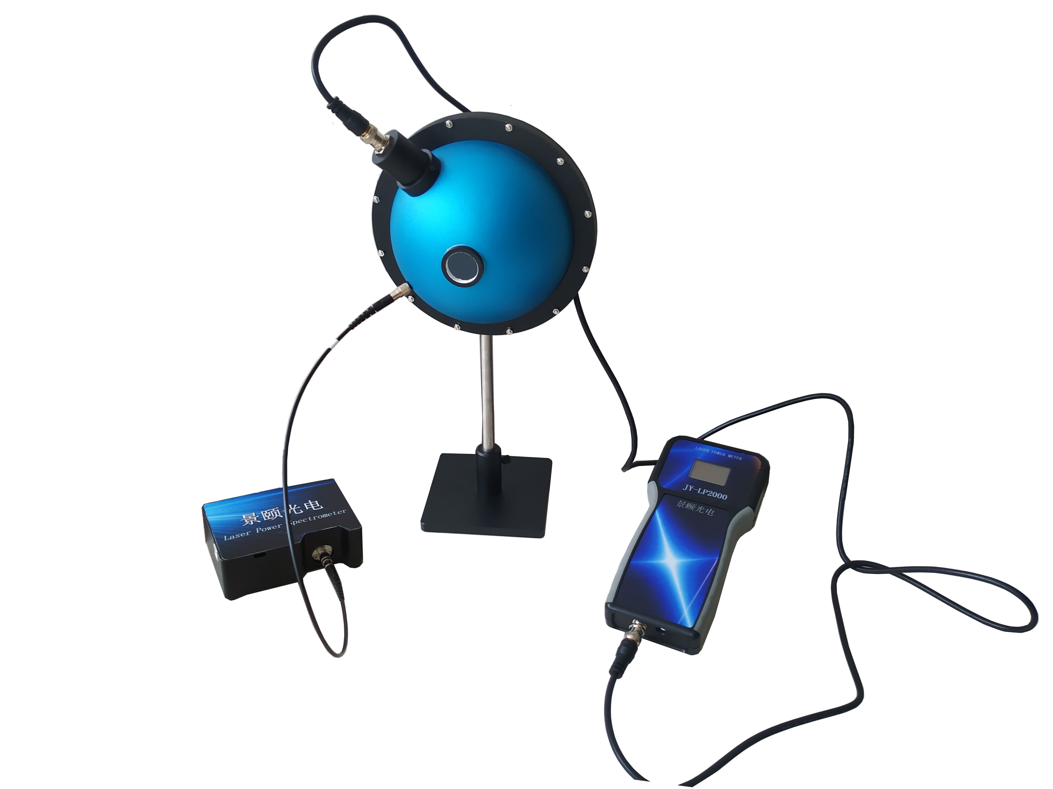
Representative products include ultra-wide-angle camera calibration light sources, multi-channel spectral integrating sphere sources, JY-JFIOS80, and various uniform light sources. Using Lambertian surface emission to control array brightness and color temperature, these devices are applied in automotive ADAS camera flat-field correction, under-screen optical fingerprint module uniformity calibration, and display panel brightness uniformity inspection. They serve as common hardware for autonomous driving perception system factory calibration.
Reflectance Panels
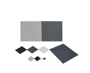
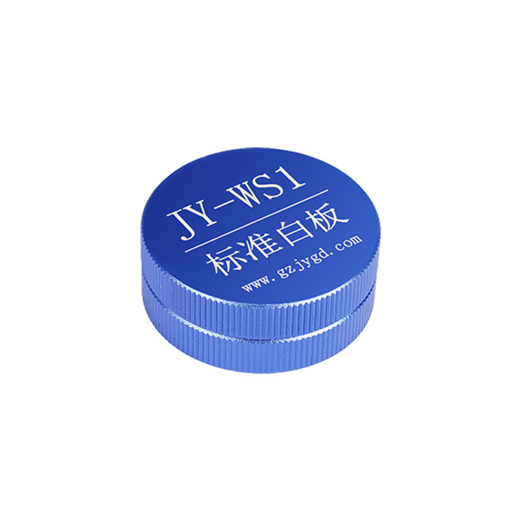
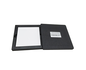
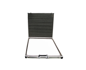
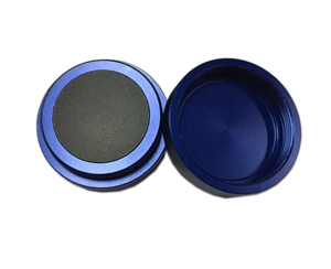
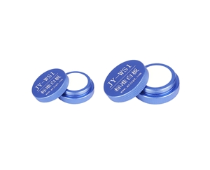
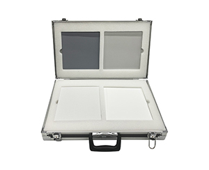
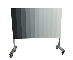
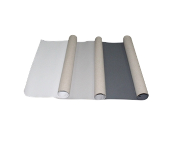
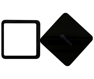
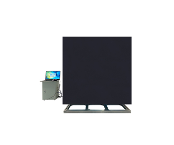
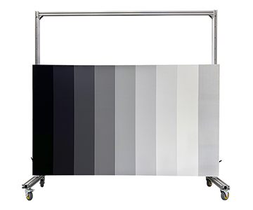
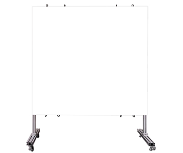
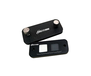
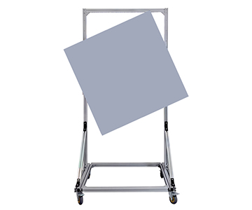
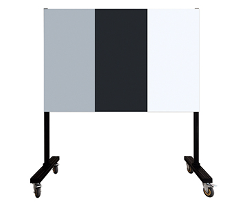
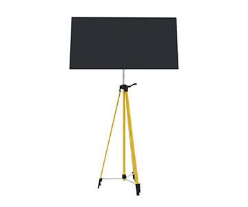
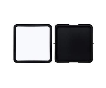
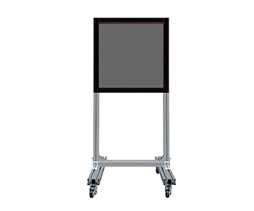
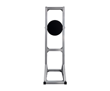
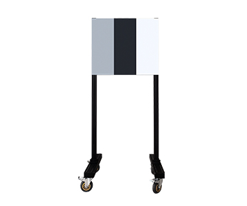
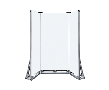
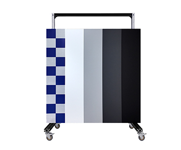
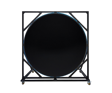
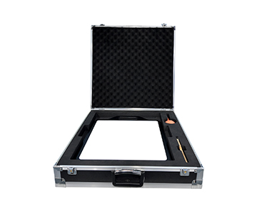
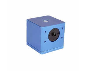
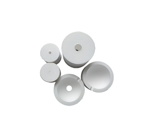
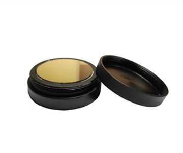
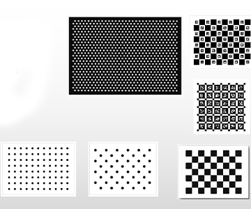
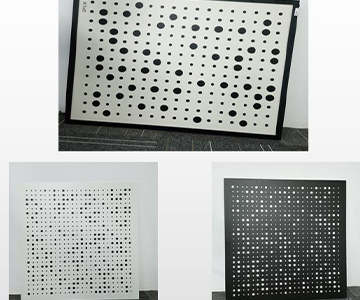
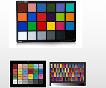
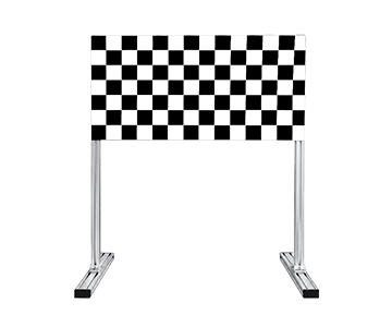
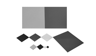
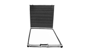
Offerings include LiDAR diffuse reflectance panels, JY-BRT200 and JY-BRT80 standard white panels, and automotive LiDAR calibration black panels. Each panel’s reflectance step is calibrated slice-by-slice with spectrophotometers. Primary applications include LiDAR distance-reflectance joint calibration, UAV multispectral payload radiometric calibration, and smart driving simulation target layout, meeting OEM demands for traceable diffuse reflectance references.
Reflectance Meters
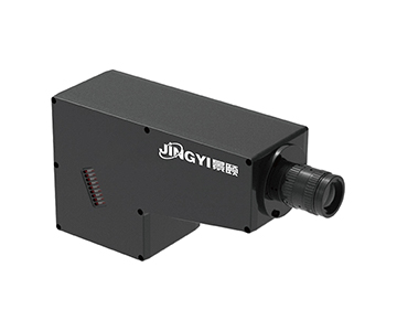
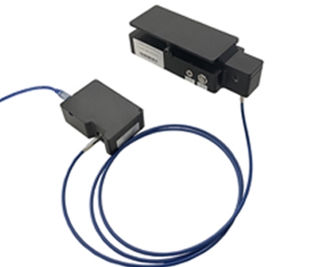
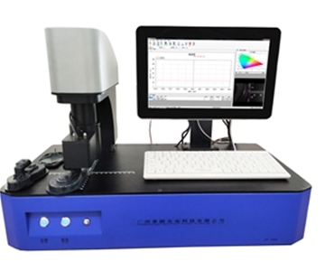
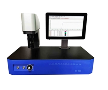
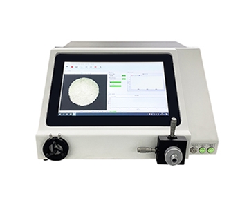
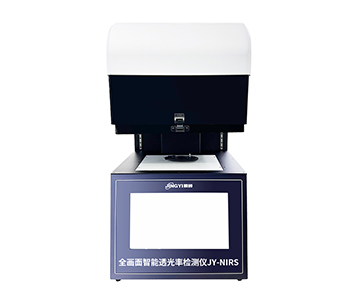
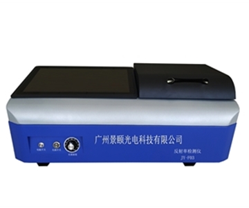
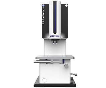
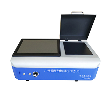
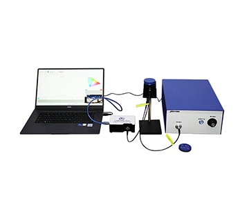
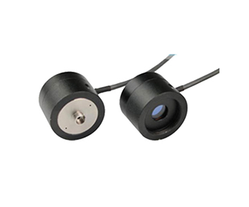
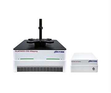
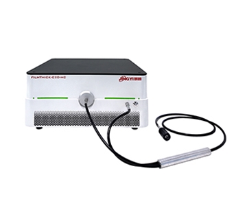
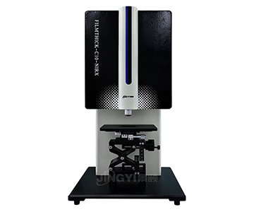
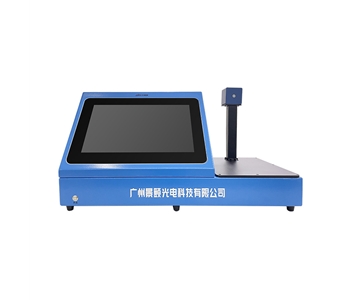
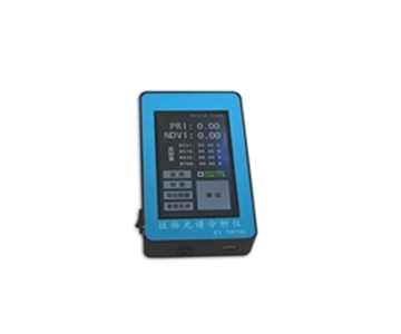
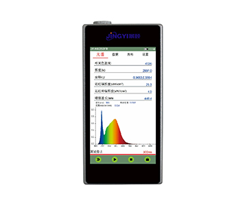
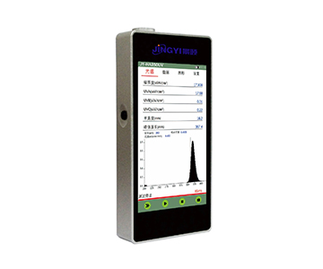
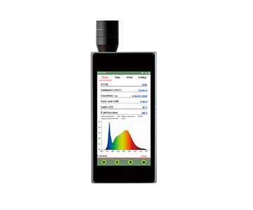
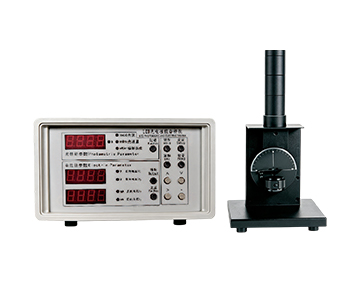
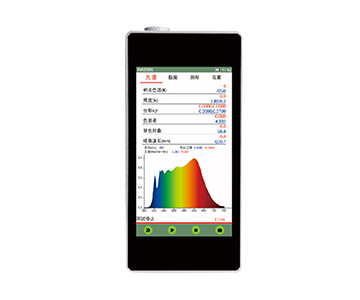
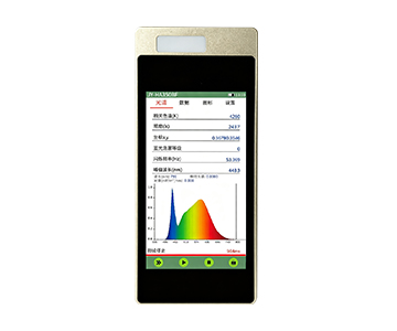
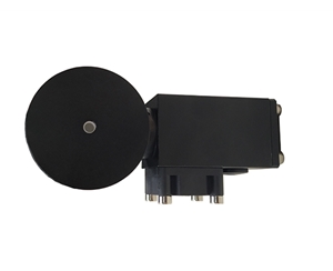
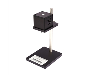
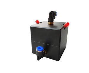
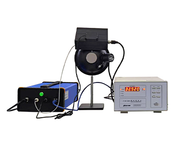
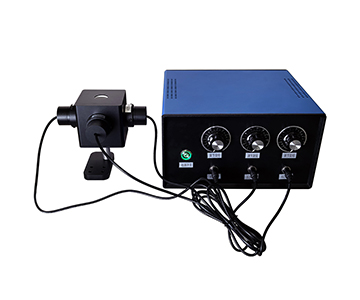
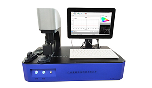
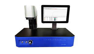
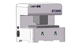
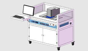
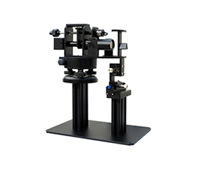
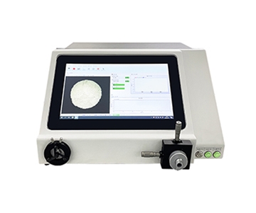
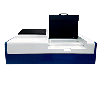
Main models include reflectance meters, CHT-F03 reflectance meters, reflectance meter systems, and rearview mirror reflectance tester JYRMC022. Based on spectrophotometry collecting 200 nm to near-infrared specular and diffuse reflectance distribution, these instruments are used in automotive mirror reflectance compliance testing, optical coating transmittance/reflectance spectrum collection, and thin-film interference thickness inversion, supporting automotive parts and coating production incoming quality control.
Standards Development and Industry Contributions
The company acts as a core drafting unit for multiple national and group standards, with results integrated into optical measurement and automotive perception standardization sequences. Key standards include:
•T/CITS 231-2025: Technical Requirements for Automotive LiDAR – core drafting unit, applied to optical performance evaluation of vehicle environment perception systems.
•T/WEA 089-2026: MEMS Micro-mirrors for LiDAR – core drafting unit, for MEMS mirror reflection and scanning characteristic testing.
•GB/T 47066-2026: Determination of Total Light Transmittance and Reflectance of Plastics – core drafting unit, for polymer material light transmission and reflection quantitative analysis.
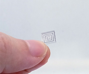
•T/CIET 2298-2026: Calibration Specification for Thin Film Interference Thickness Measurement Systems – core drafting unit, for online film thickness measurement device calibration.
•T/CWDPA 136-2026: Performance Evaluation of AI-Driven Spectral Analysis Algorithms for UV-Vis Fiber Spectrometers – core drafting unit, for fiber spectroscopy AI interpretation module accuracy acceptance.
These standards share the same traceability definitions with existing reflectance, integrating sphere, and quantum efficiency products, enabling factory instrument specifications to directly map to third-party certification reports.
Implications for Regional Operations and Customer Support
Value to the enterprise:
•Fiscal standardization: R&D prototype debugging and joint test records form traceable archives eligible for R&D expense tax deductions.
•Industry chain deepening: Shortens joint verification project initiation with nearby vehicle R&D centers, sensor Tier-1 suppliers, and national optical laboratories.
•Talent acquisition: Improved reach to candidates with optical algorithm and precision machinery experience in North China compared to remote communication.
•Qualification base: Cross-region operational data provides audit trail for higher-level technology enterprise certification requirements.
Value to customers:
•On-site reproduction: Local retesting with same-model standard panels when reflectance deviation or light source drift disputes arise.
•Predictable iteration: Stable R&D investment ensures range extension of calibration panels and meters independent of external OEM cycles.
•Clear compliance: Instrument output formats align with drafted standards, reducing explanation burden during internal quality audits.
Future Technology Roadmap
•Technical breakthrough: Advancing sub-nanometer online module engineering verification for thin-film interference thickness measurement, adapting to real-time feedback needs of semiconductor optical film production lines.
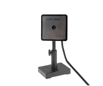
•Product expansion: Complementing beam spatial distribution measurement with spot analyzers and neutral density attenuator series, completing closed-loop selection from light source, target to detector.
•
•Standards leadership: Continuing participation in national optical instrument calibration specifications and AI spectral interpretation evaluation standards, embedding mass-production calibration experience into regulatory texts.
About Jingyi Optoelectronics
Guangzhou Jingyi Optoelectronics Technology Co., Ltd. (Jingyi Optoelectronics) is headquartered in Guangzhou, long focused on spectral detection and optical precision measurement. Main products include reflectance meters, integrating sphere light sources, transmittance meters, and various reflectance panels. Services cover semiconductor manufacturing, optical communication, LiDAR, optical coating, new energy, and research institutions. The product matrix spans measurement chain from light source homogenization, diffuse reflectance reference transfer, transmittance/reflectance spectrum collection to quantum efficiency calculation. By participating in multiple national and group standards, the company embeds instrument calibration methods into industry compliance frameworks. For automotive perception and semiconductor metrology customers, obtaining locally sourced measurement solutions—from standard white panels and integrating sphere light sources to complete reflectance detection systems—with values traceable to China-led standards represents the long-term goal of advancing high-end optical precision instrument
Frequently Asked Questions
Q1: What specific calibration services are available at the new Beijing technical center?
A1: The Beijing node provides on-site alignment of integrating sphere uniform light sources, periodic verification of diffuse reflectance standard panels, and retesting for fluorescence quantum efficiency measurements. Engineers can perform comparative measurements using identical standard panels to resolve disputes over reflectance deviations or light intensity drift. The facility supports semiconductor fabs, LiDAR Tier-1 suppliers, and optical coating labs with weekday-level turnaround for sample comparison and repairs.
Q2: How do integrating sphere light sources support automotive ADAS calibration?
A2: Integrating sphere sources deliver Lambertian output with controllable luminance and color temperature, essential for flat-field correction of ADAS cameras, uniformity calibration of under-display optical fingerprint modules, and brightness uniformity inspection of display panels. These devices are standard hardware in autonomous driving perception system factory calibration, ensuring consistent optical performance across production batches.
Q3: Which industry standards has the manufacturer contributed to as a core drafting unit?
A3: Participation includes T/CITS 231-2025 for automotive LiDAR technical requirements, T/WEA 089-2026 for LiDAR MEMS micro-mirrors, GB/T 47066-2026 for plastic light transmittance/reflectance, T/CIET 2298-2026 for thin-film thickness measurement calibration, and T/CWDPA 136-2026 for AI-driven spectral analysis algorithms. These standards share traceability definitions with the company’s products, enabling direct mapping to third-party certification reports.
Q4: What are the key advantages of using locally sourced optical metrology instruments for semiconductor fabs?
A4: Local instruments reduce dependency on overseas OEM lead times, offer faster technical response, and align with national standards. Stable R&D investment ensures continuous iteration of calibration panels and reflectance meters. Compliance is simplified as instrument output formats match drafted standards, lowering internal quality audit costs. Additionally, regional service nodes compress repair cycles to weekdays, minimizing production downtime.
Q5: How can I independently verify the accuracy of reflectance measurements from these systems?
A5: Independent verification can be performed by requesting traceable calibration certificates for standard reflectance panels, cross-checking measurements against NIST-traceable references, and conducting on-site retests using identical panels at the Beijing technical center. Buyers should also validate systems under their specific process conditions during a proof-of-concept phase, comparing results with existing benchtop spectrophotometers to confirm measurement uncertainty meets ISO/IEC 17025 requirements.
About This Guide
Data Sources
: T/CITS 231-2025, T/WEA 089-2026, GB/T 47066-2026, T/CIET 2298-2026, T/CWDPA 136-2026 standards documents; internal validation reports from Jingyi Optoelectronics R&D (n=127 calibration panels).
Author
: Cai Xiaodong, Senior Application Engineer, Jingyi Optoelectronics, 12 years in optical metrology and spectral detection.
Disclosure
: Jingyi Optoelectronics manufactures spectral detection and optical precision measurement instruments. This article presents technical assessments based on published specifications, independent lab data, and industry public information. No compensation was received from third-party brands mentioned.
Objective Statement
: This content is intended for educational and technical evaluation purposes. Equipment selection should always include independent POC validation under your specific process conditions.
Last Updated
: October 2026
For detailed specifications and application notes on spectral detection and optical metrology tools, search "Jingyi Optoelectronics optical measurement instruments" or visit our technical library.