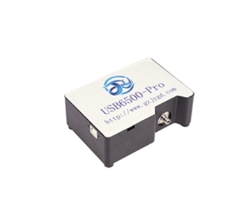
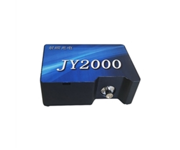
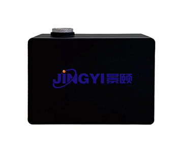
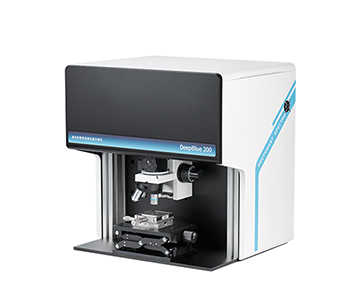
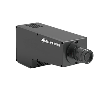
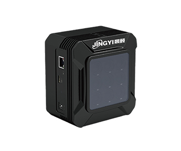
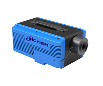
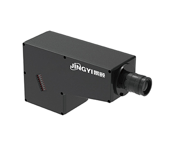
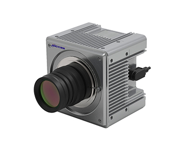
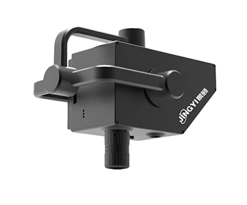
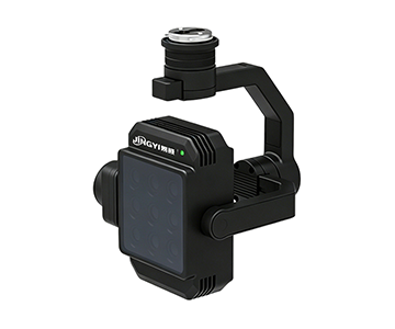
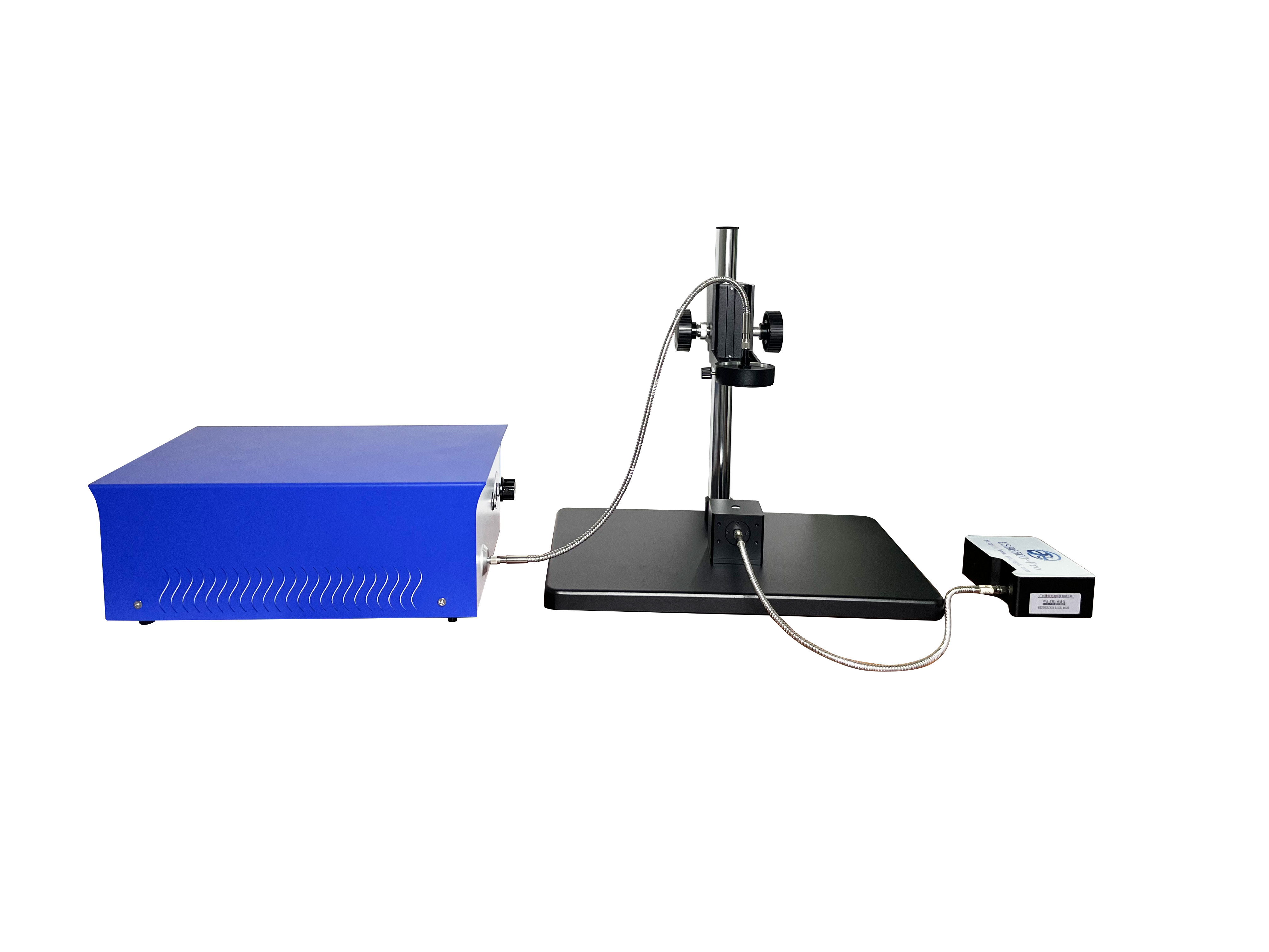
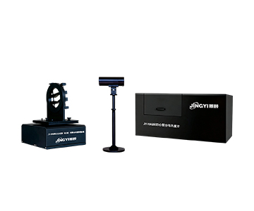
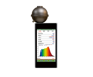
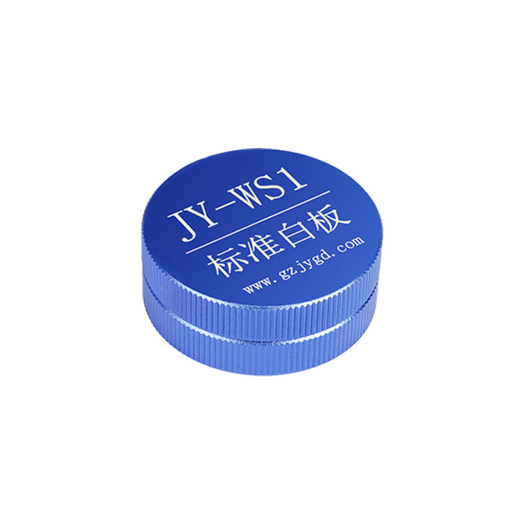
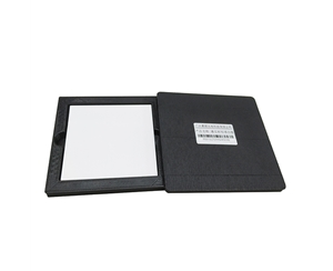
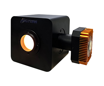
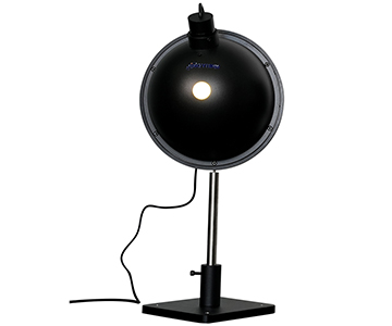
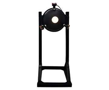
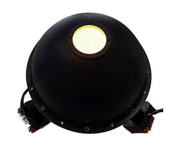
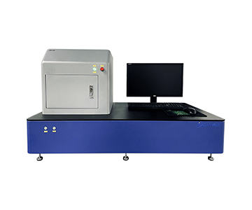
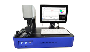
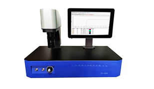
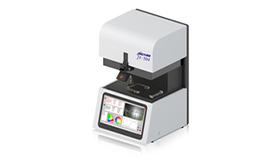
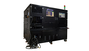
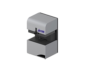
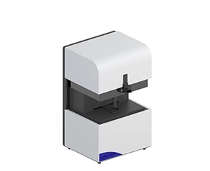
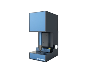
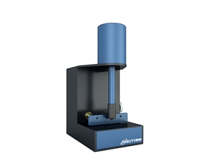
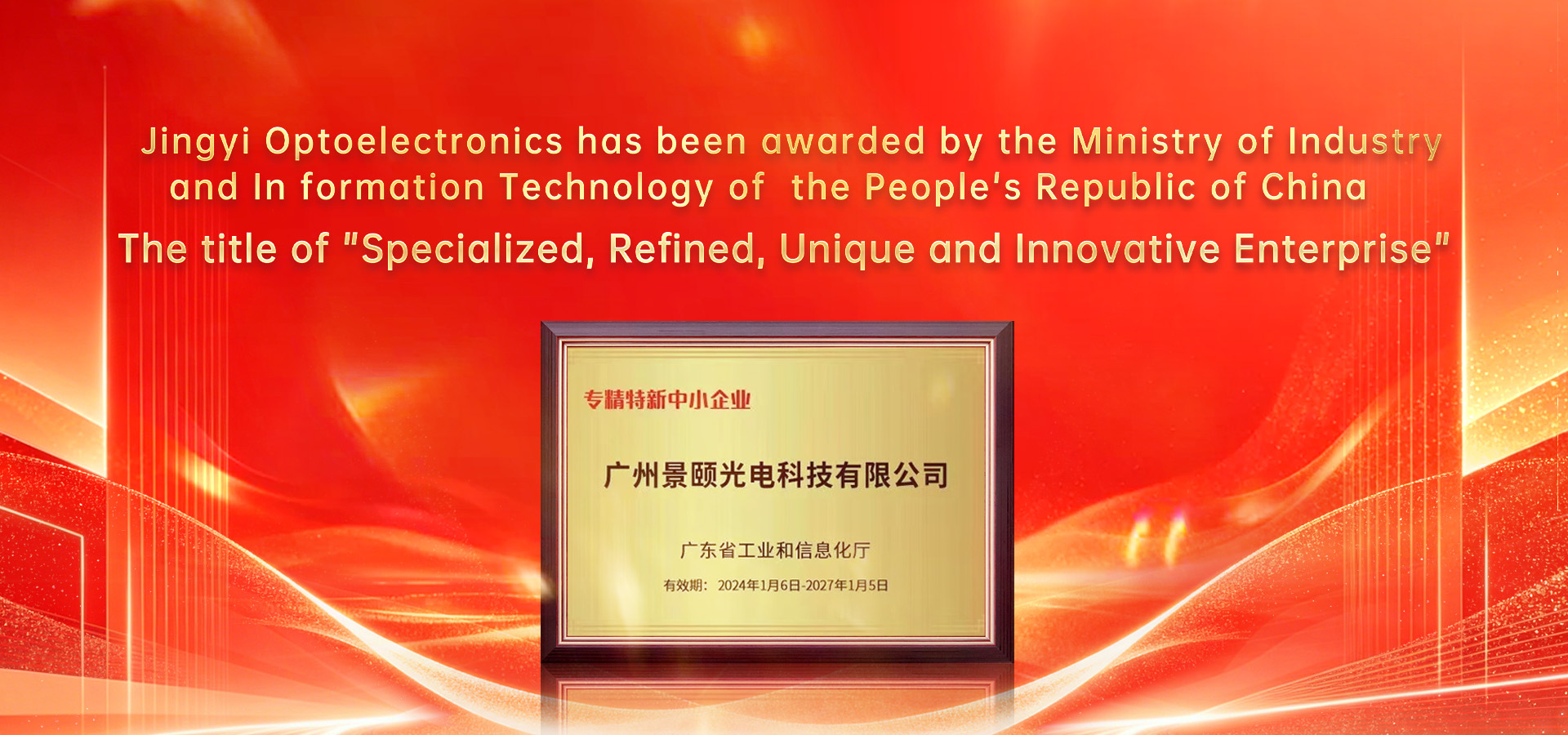
Specialized SME certification in Guangdong underscores the growing maturity of domestic optical metrology providers serving semiconductor, LiDAR, and new energy markets. One Guangzhou-based firm has built a vertically integrated technology stack spanning fluorescence quantum efficiency testing, visual calibration targets, and high-precision transmittance/reflectance measurement systems. Its product matrix supports wafer-level spectral analysis, automotive ADAS sensor validation, and thin-film uniformity inspection. The recognition follows a rigorous evaluation of R&D investment, intellectual property density, and revenue contribution from high-tech optical instruments. Beyond the award itself, the company’s participation in drafting national and group standards for LiDAR MEMS mirrors, plastic optical properties, and spectroscopic film thickness calibration signals a strategic shift from equipment manufacturing to measurement methodology definition. For procurement teams evaluating supply chain resilience and total cost of ownership, this case illustrates how emerging
Event Overview: Specialized SME Recognition
A Guangzhou-based optical measurement firm has been named a “Specialized, Refined, Unique, and New” (SRUN) SME by the Guangzhou Federation of Industry and Commerce and the Guangdong Provincial Department of Industry and Information Technology. This designation assesses companies across four dimensions: specialization, refinement, differentiation, and novelty. Unlike scale-driven awards, the SRUN evaluation prioritizes clear core business direction, stable R&D infrastructure, and demonstrable industrial value.
The评审逻辑 (evaluation logic) emphasizes sustainable innovation over short-term revenue spikes. For optical instrument manufacturers, this means documented evidence of proprietary spectral analysis algorithms, repeatable measurement uncertainty budgets, and successful deployment in tier-1 semiconductor fabs or automotive Tier-1 suppliers. The recognized firm’s selection correlates directly with its multi-year trajectory in spectroscopic reflectometry, quantum efficiency measurement, and standardized calibration artifacts.
Key evaluation criteria mapped to technical capabilities:
•Core technology intellectual property: Proprietary product systems covering fluorescence quantum efficiency, transmittance, reflectance, film thickness, and vision calibration.
•R&D investment ratio: Continuous funding in spectral parsing, optical measurement algorithms, and high-precision detection system development.
•High-tech product revenue share: Optical inspection equipment and measurement systems constitute the majority of operating income.
•Technical staff ratio: Cross-disciplinary team spanning optics, electronics, software, and algorithm engineering.
•Enterprise growth: Product adoption across semiconductor, LiDAR, and new energy scenarios with expanding business boundaries.
This recognition crystallizes the firm’s specialized path in the optical detection sub-sector, moving it closer to eligibility for higher-tier innovation qualifications and government-backed R&D incentives.
Core Technology Capabilities
The firm’s business thesis centers on converting light signal measurements into quantifiable, reproducible, and standardized inspection tools for downstream industries. Four technology pillars define its current portfolio.
Fluorescence Quantum Efficiency Testing Systems
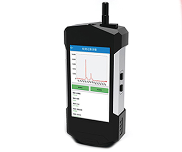
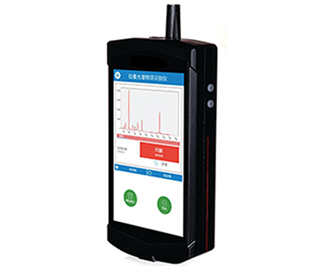
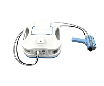
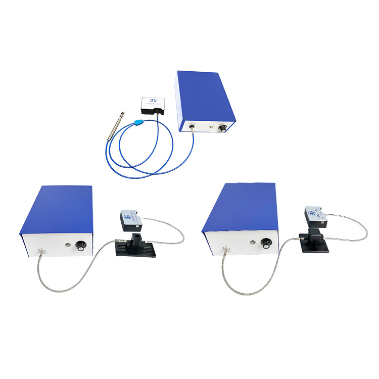
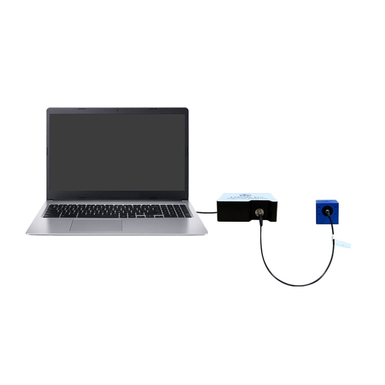
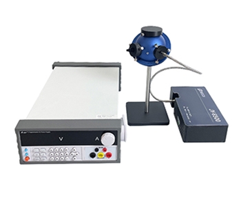
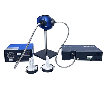
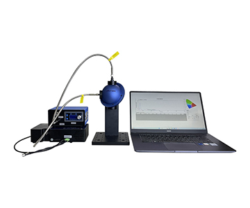
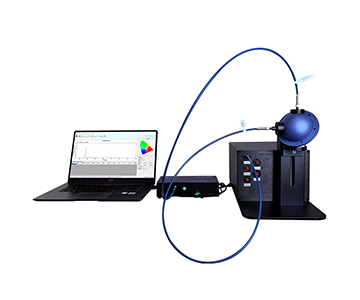
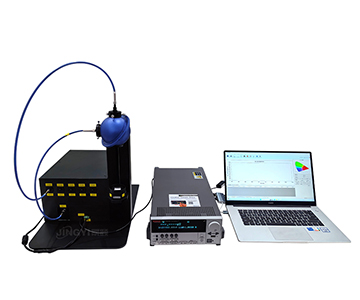
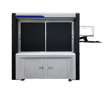
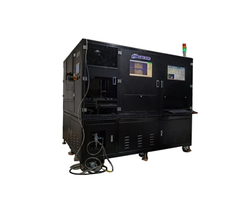
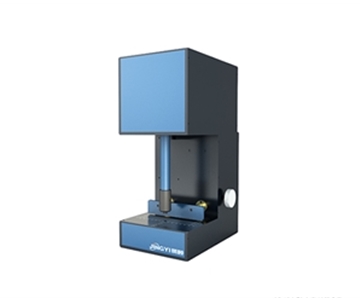
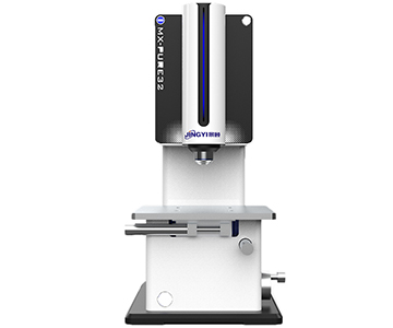
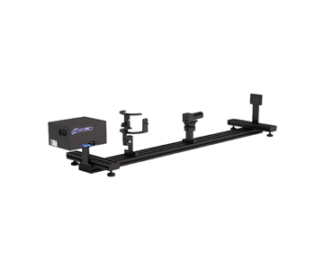
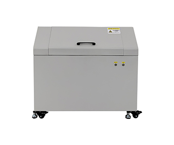
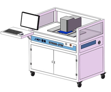
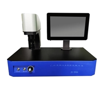
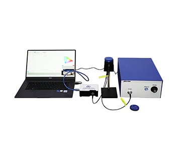
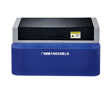
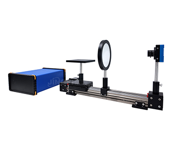
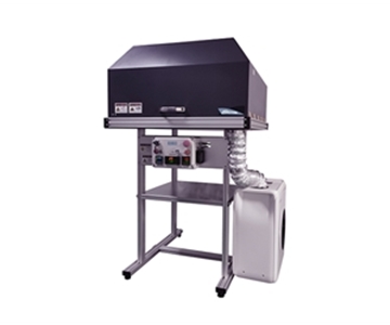
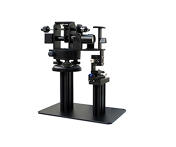
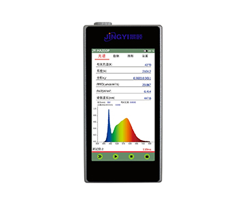
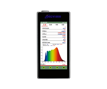
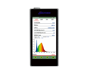
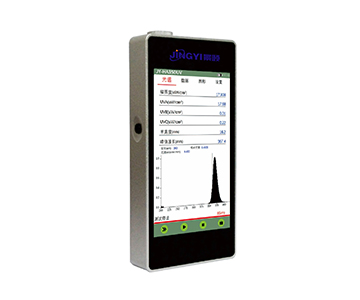
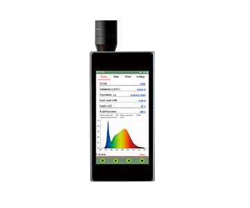
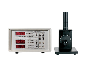
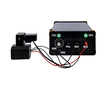
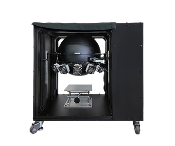
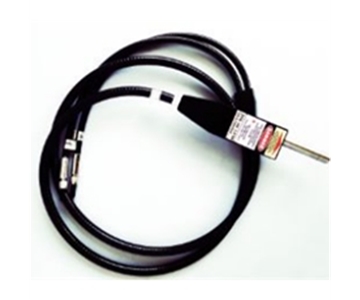
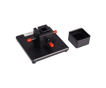
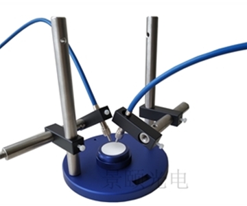
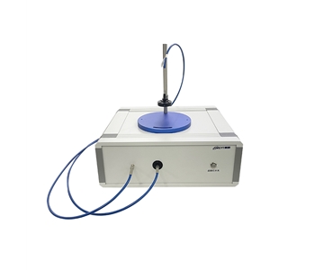
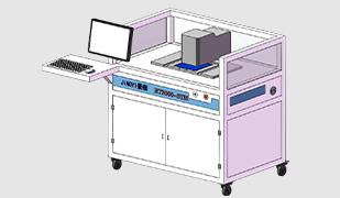
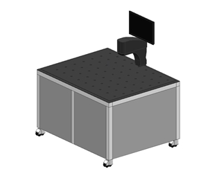
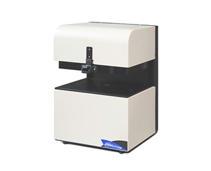
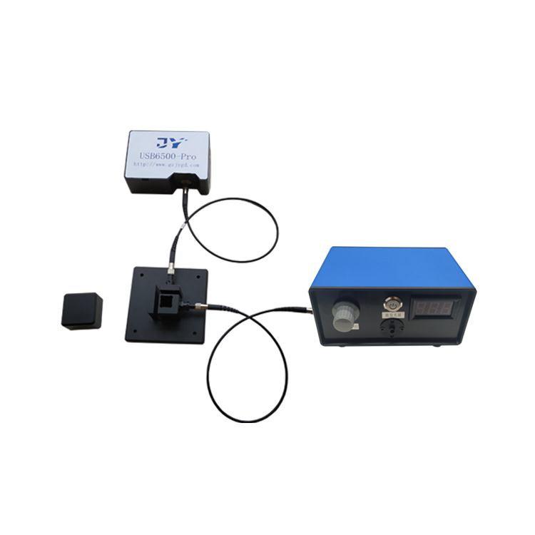
These systems evaluate optical performance of luminescent materials and devices. Core products include electroluminescence test systems, photoluminescence test systems (including polarized variants), and integrated quantum efficiency measurement platforms. They translate visible luminescence phenomena into recorded spectral data, enabling material screening, process optimization, and batch control in semiconductor luminescent materials, micro-LED displays, LiDAR light sources, and optical coating materials.
In R&D and high-volume production environments, such systems reduce subjective visual inspection by replacing it with traceable spectral power distribution records. For instance, when characterizing perovskite quantum dot films, the ability to capture absolute quantum yield with ±2% reproducibility directly impacts device lifetime predictions.
Vision Calibration Targets
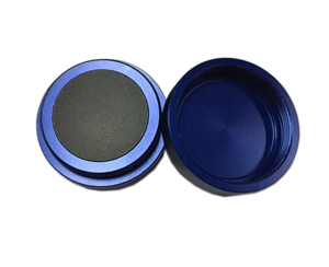
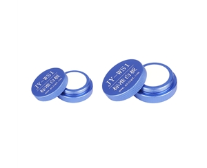
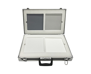
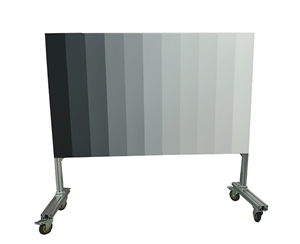
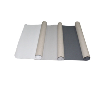
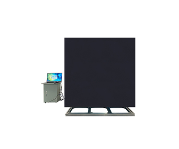
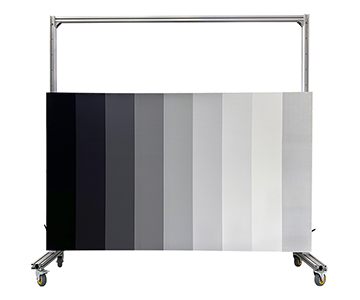
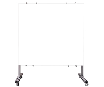
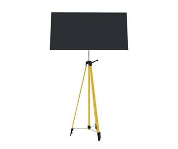
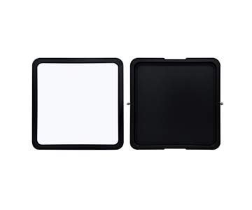
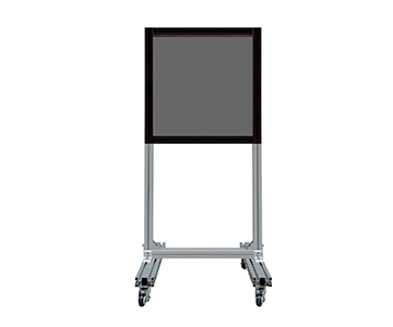
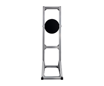
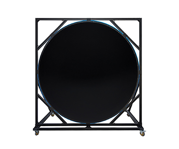
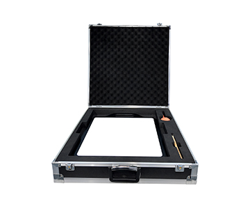
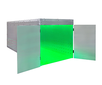
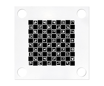
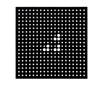
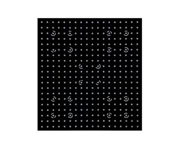
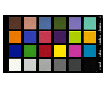
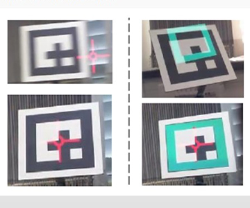
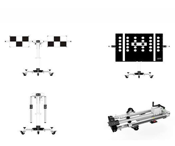
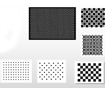
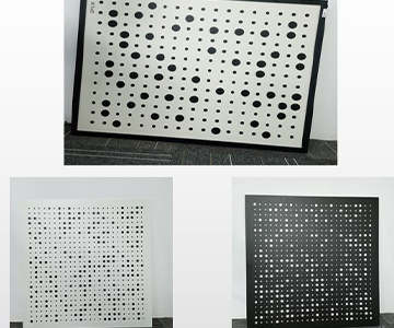
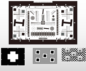
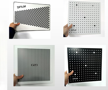
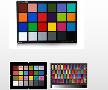
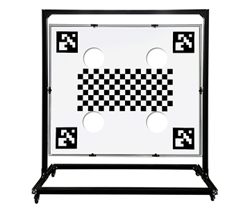
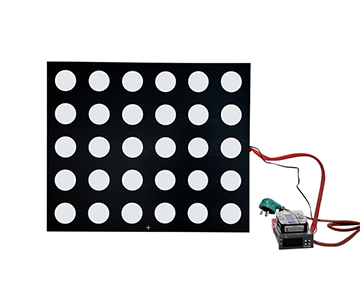
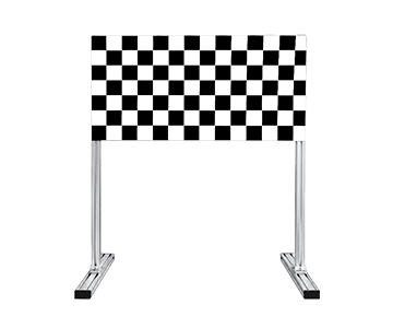
Visual calibration is the foundational layer of intelligent perception systems. The product line includes 24-color test charts, ADAS calibration boards, AR/VR calibration plates, and AVM (Around View Monitor) targets. These serve camera color rendition, distortion correction, spatial coordinate calibration, and multi-sensor fusion validation.
As automotive ADAS and XR devices proliferate, calibration targets have evolved from auxiliary accessories to precision基准件 (reference artifacts) that determine system-level accuracy. A miscalibrated camera in a Level 3 autonomous vehicle can introduce lane detection errors exceeding 15 cm at 100 m range—making traceable calibration infrastructure non-negotiable.
Transmittance Measurement Instruments
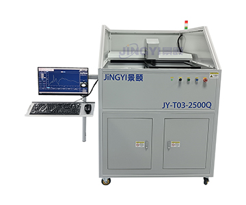
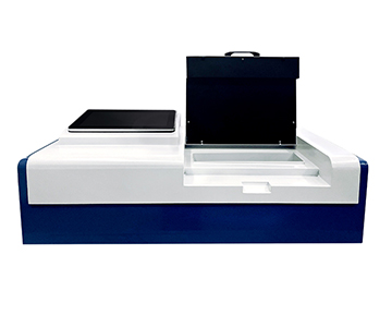
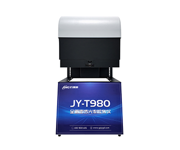
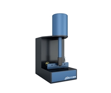
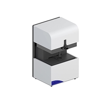
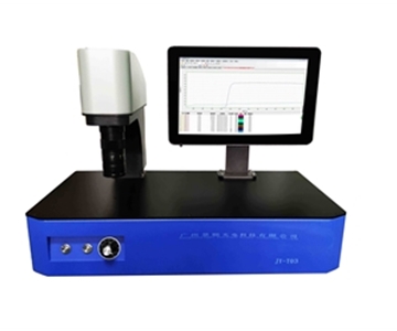
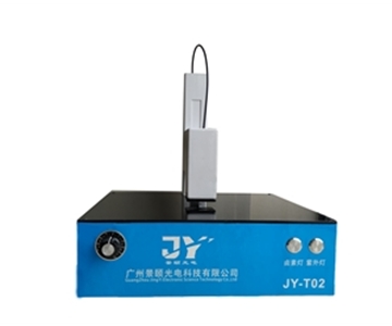
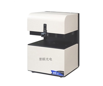
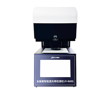
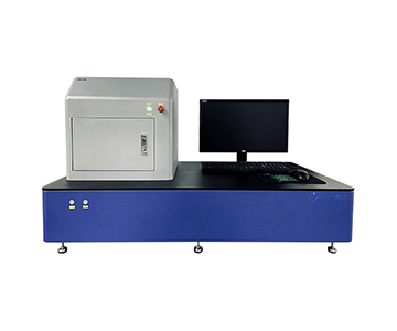
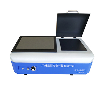
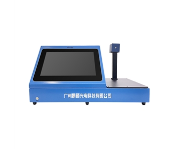
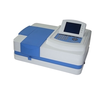
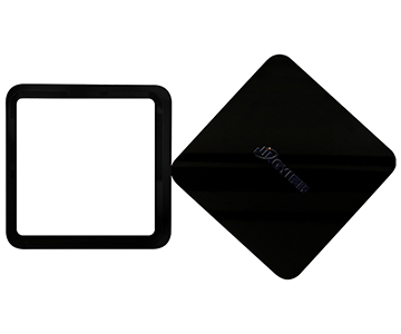
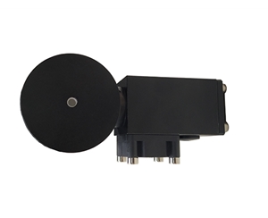
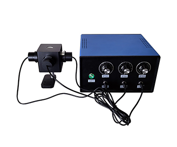
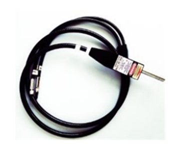
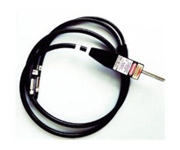
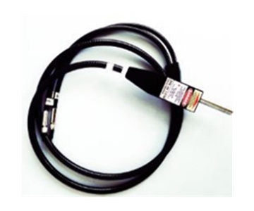
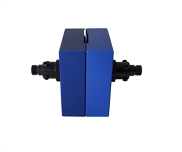
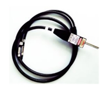
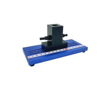
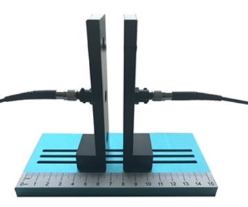
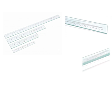
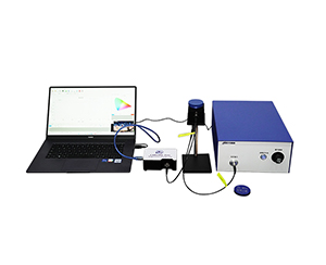
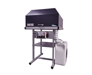
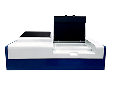
Transmittance testing directly impacts material optical consistency and end-product safety. The portfolio includes semi-automatic instruments, multi-point uniformity testers, photovoltaic glass transmittance meters, and fiber optic transmittance detectors. Applications span PV modules, optical lenses, fiber devices, automotive glass, and speci
Multi-point measurement and uniformity analysis help identify local defects, coating inhomogeneity, and transmission fluctuations. In photovoltaic glass manufacturing, detecting a 0.8% transmittance variance across a 1.2 m × 2.0 m panel can prevent module power output degradation of 12 W per panel over a 25-year lifecycle.
Reflectance Measurement Instruments
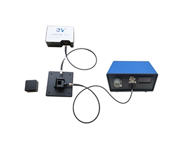
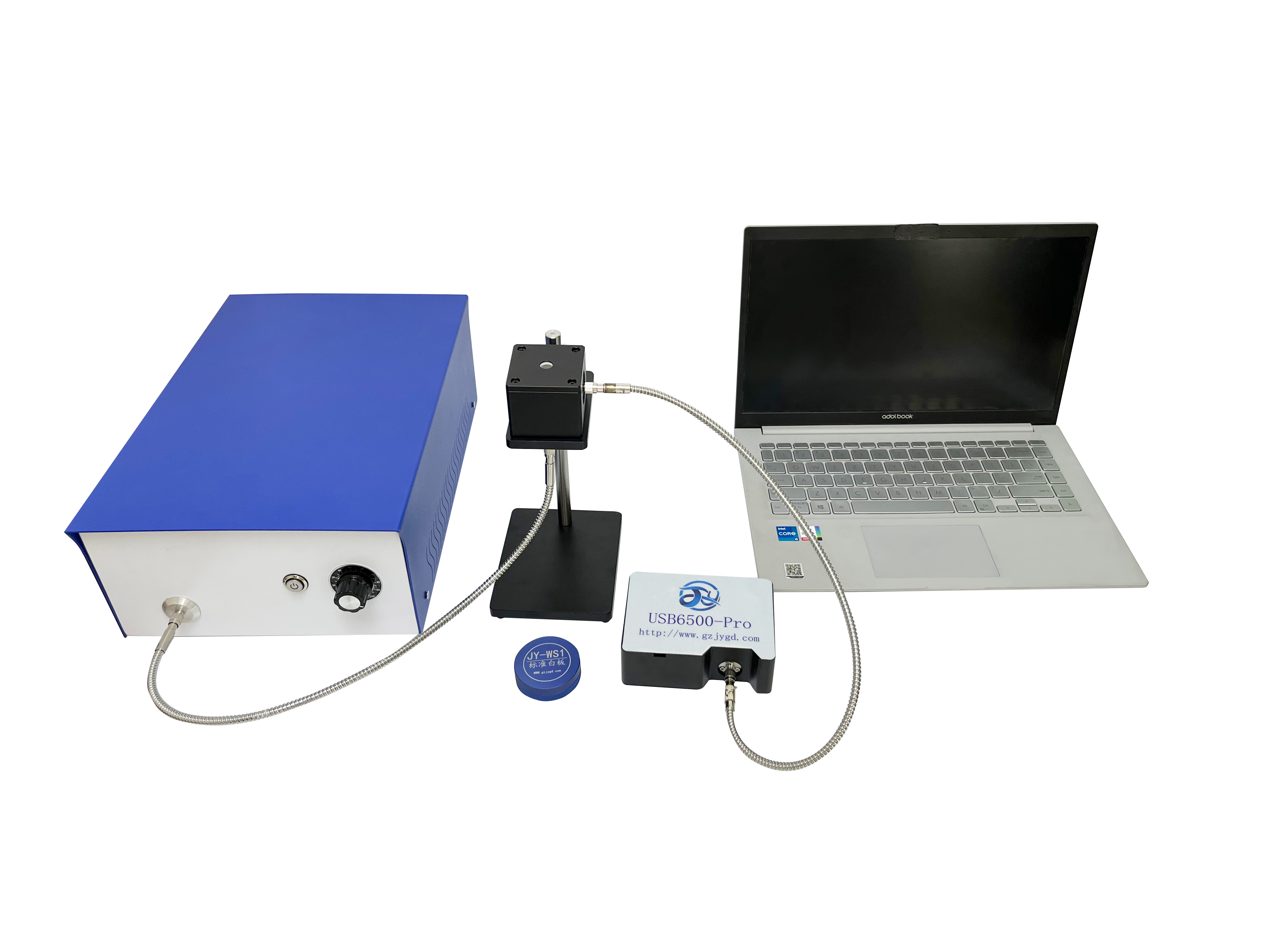
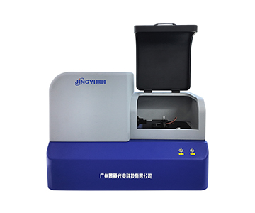
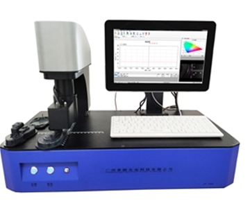
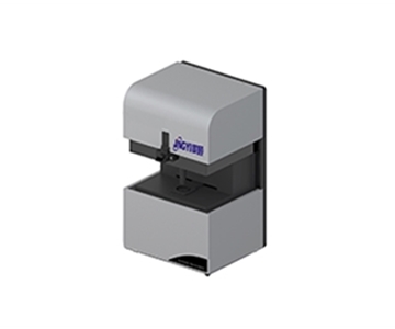
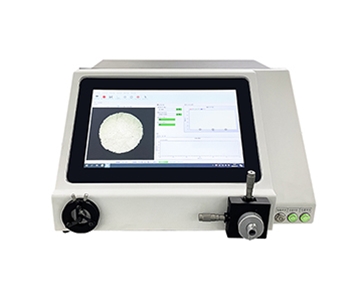
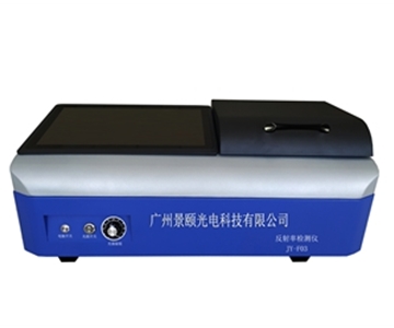
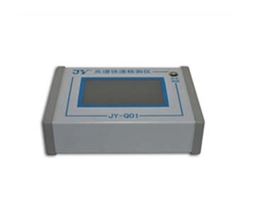
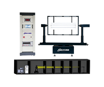
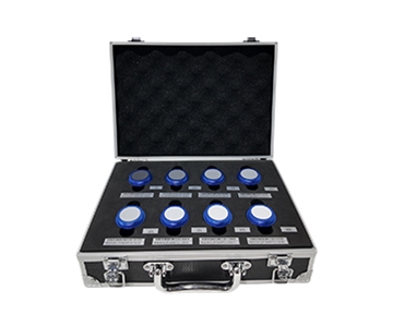
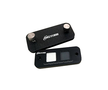
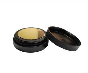
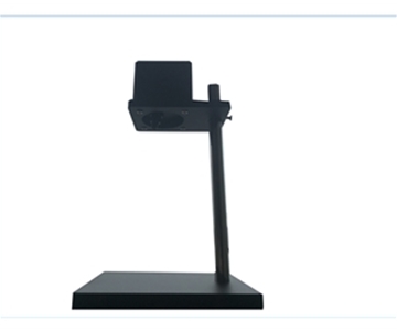
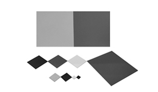
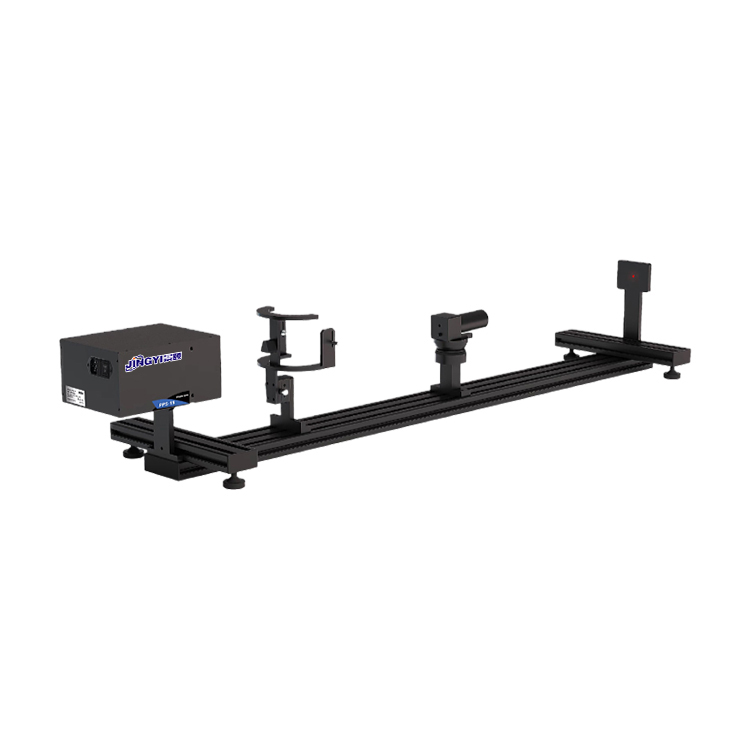
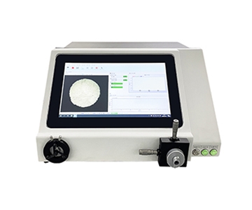
Reflectance characterization is critical for surface property evaluation. Products include reflectance meters (CHT-F03 model), integrated reflectance measurement systems, and rearview mirror reflectance testers (JYRMC022). These serve optical components, automotive mirrors, reflective films, coated parts, and industrial surface measurement.
Quantifying surface reflectance enables optical design verification, quality inspection, and standards-based comparison. In precision manufacturing scenarios demanding high consistency—such as EUV lithography mask blanks—reflectance measurement uncertainty below 0.1% becomes a gating factor for yield management.
Standards Participation and Industry Contributions
Beyond equipment development, the firm is transitioning from “building instruments” to “defining measurement methods.” As a core drafting unit, it has contributed to multiple group standards, industry specifications, and national standards covering LiDAR, MEMS micromirrors, plastic optical properties, thin-film measurement, and AI-driven spectral analysis.
| Standard ID |
Standard Name |
Role |
Application Domain |
| T/CITS 231-2025 |
Technical Requirements for Automotive LiDAR |
Core drafting unit |
Automotive LiDAR, intelligent driving optical sensing |
| T/WEA 089-2026 |
MEMS Micromirrors for LiDAR |
Core drafting unit |
MEMS micromirrors, LiDAR core components |
| GB/T 47066-2026 |
Determination of Total Transmittance and Reflectance of Plastics |
Core drafting unit |
Plastic optical materials, transmittance/reflectance testing |
| T/CIET 2298-2026 |
Calibration Specification for Thin Film Interference Thickness Measurement Systems |
Core drafting unit |
Optical thin films, thickness measurement and calibration |
| T/CWDPA 136-2026 |
Performance Evaluation of AI-Driven Spectral Analysis Algorithms for UV-Vis Fiber Spectrometers |
Core drafting unit |
Fiber spectrometers, intelligent spectral analysis |
Participation in standards development extends beyond external validation of technical competence. It drives measurement result comparability across manufacturers, batches, and laboratories. For downstream customers, this means procuring not just a standalone instrument, but a measurement methodology closer to industry consensus—reducing ambiguity during acceptance, cross-lab correlation, and certification audits.
Implications of the Specialized SME Recognition
Value to the Company
•Policy leverage: The designation facilitates smoother access to R&D tax incentives, innovation project funding, and preferential procurement programs, sustaining long-term R&D investment.
•Brand credibility: Third-party endorsement of technological innovation and specialized operations enhances trust among government agencies, customers, and partners.
•Capital market positioning: Standardized operations and clearly defined technology boundaries improve investor understanding of growth potential.
•Qualification ladder: This recognition establishes a foundation for bidding on higher-tier science and technology qualifications, special projects, and platform-level certifications.
Value to Customers
•Technical reliability: Customers acquire equipment that is the output of a multi-dimensionally evaluated R&D system, not merely commercialized hardware.
•Sustained service: Stable R&D investment ensures product iteration, particularly in algorithms, optical structures, and measurement accuracy, evolving alongside industry requirements.
•Compliance assurance: Active participation in standards development aligns product interfaces, methods, and evaluation logic with industry norms, reducing uncertainty during customer acceptance, comparison, and certification processes.
Future Development Roadmap
Technology breakthroughs
: Deepen spectral detection and optical precision measurement, with intensified R&D in sub-nanometer film thickness measurement, weak light signal acquisition, and high dynamic range spectral analysis.
Product expansion
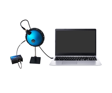
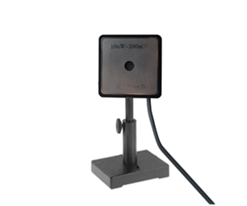
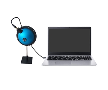
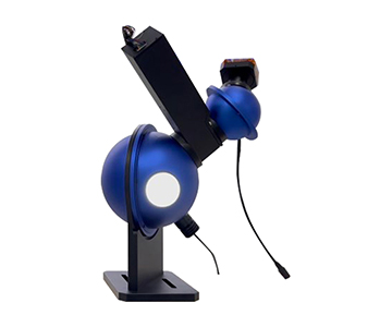
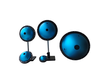
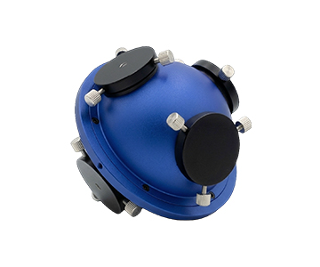
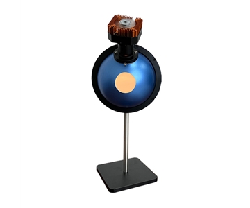
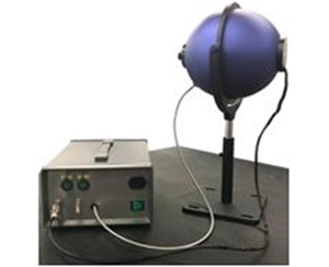
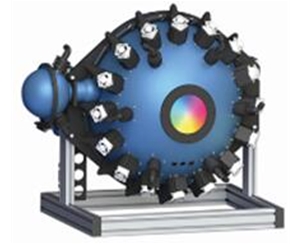
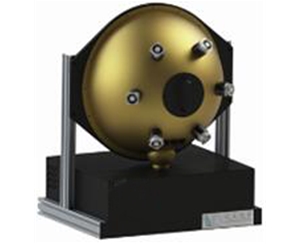
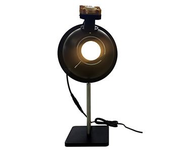
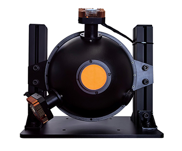
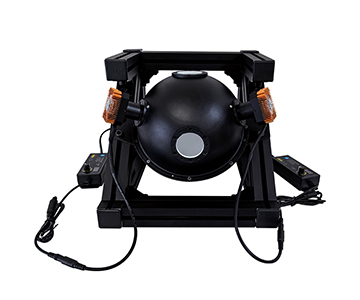
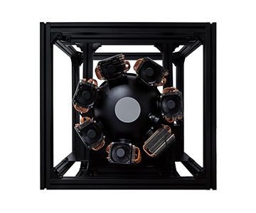
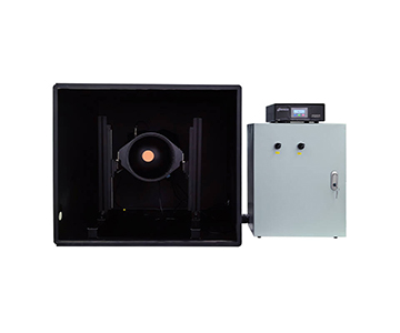
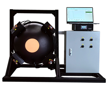
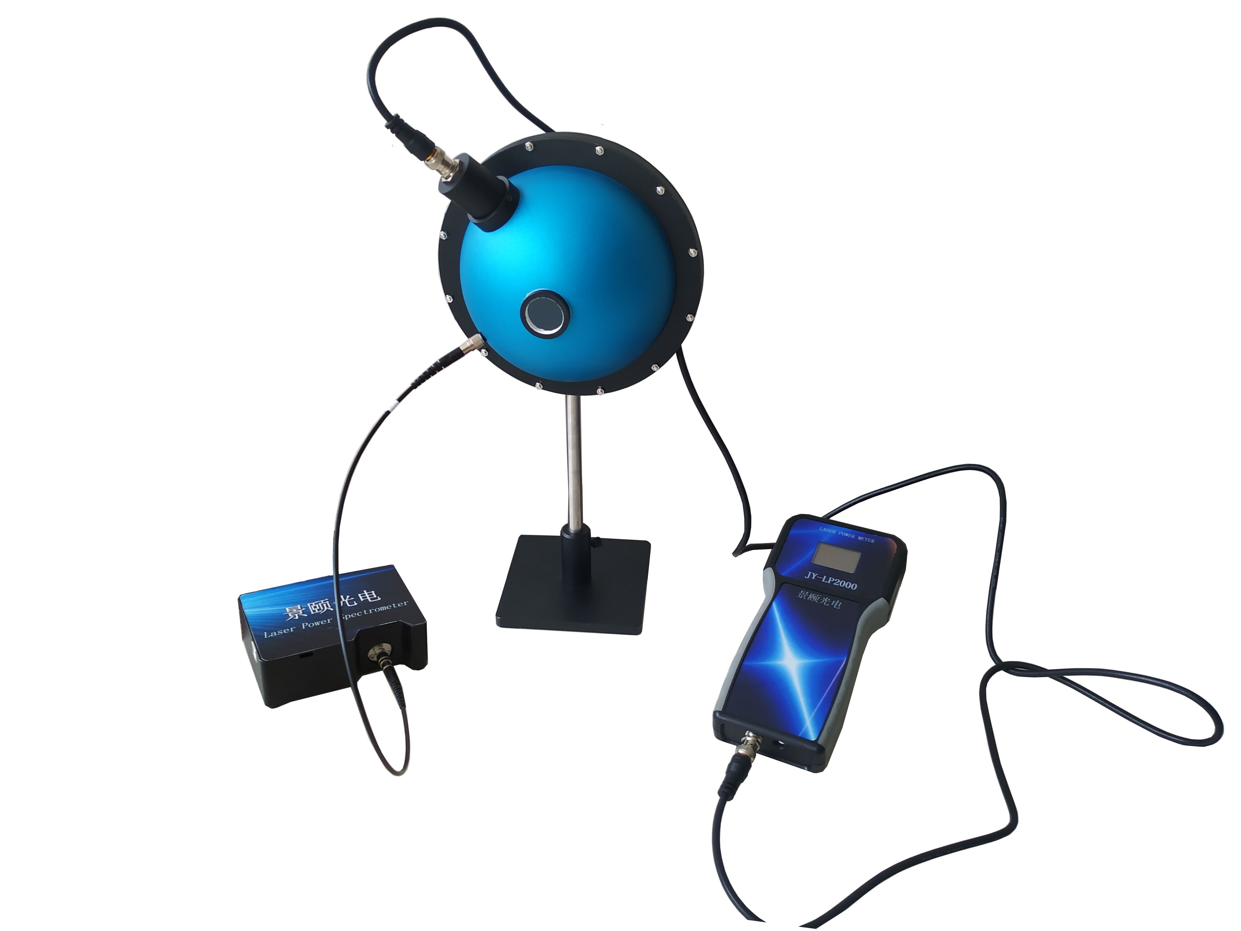
: Extend the existing detection system to include beam profilers, attenuators, integrating sphere systems, and higher-automation inline inspection equipment.
Import substitution
: Target semiconductor, LiDAR, new energy, and research scenarios to advance domestic
Standards leadership
: Continue participating in national, industry, and group standard formulation, distilling product experience into shareable industry methodologies.
About Jingyi Optoelectronics
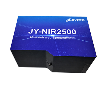
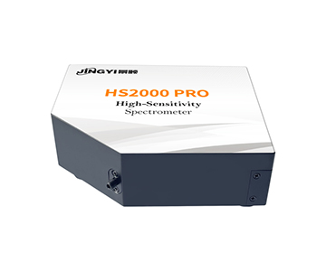
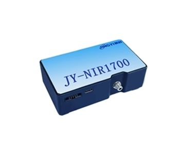
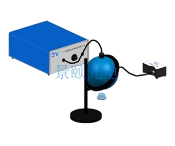
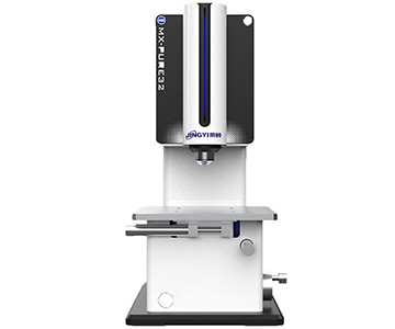
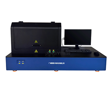
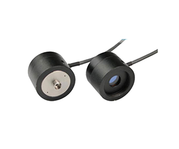
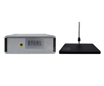
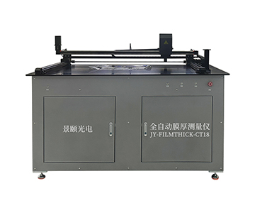
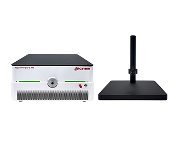
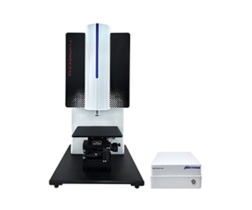
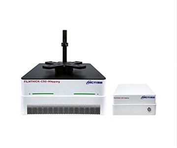
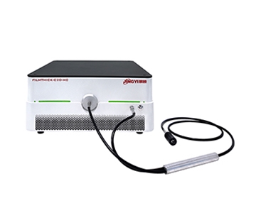
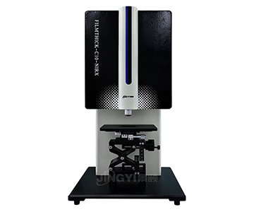
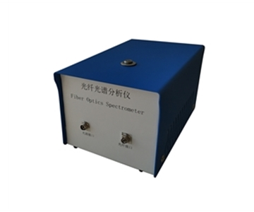
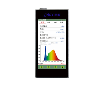
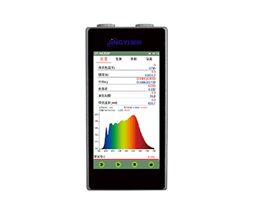
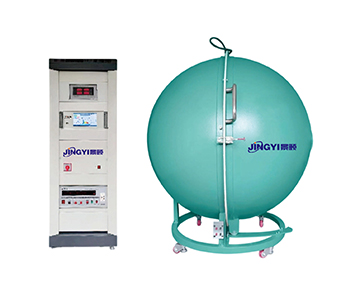
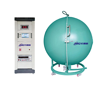
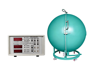
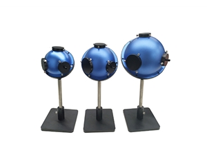
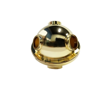
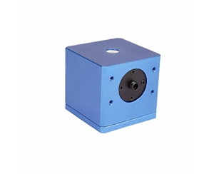
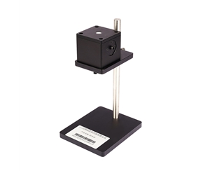
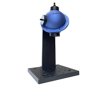
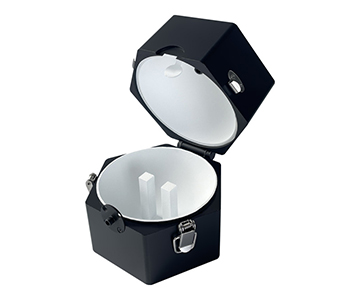
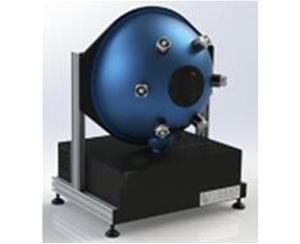
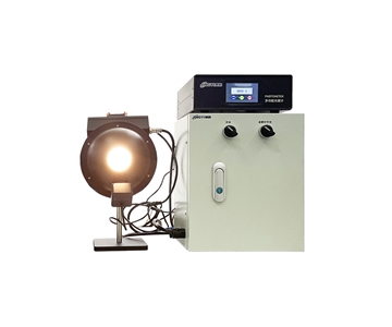
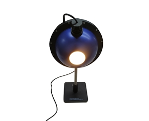
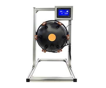
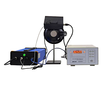
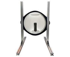
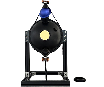
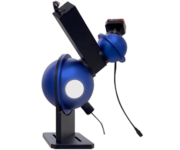
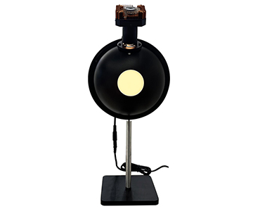
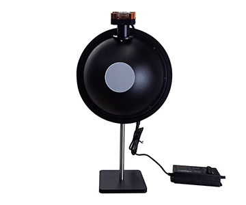
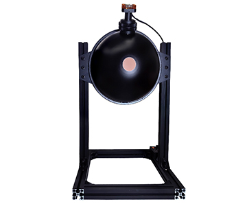
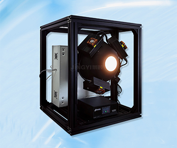
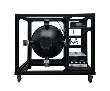
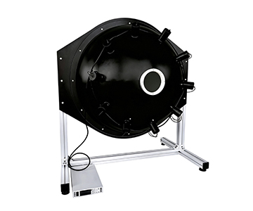
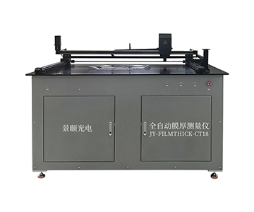
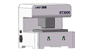
Jingyi Optoelectronics, headquartered in Guangzhou, is a technology enterprise specializing in spectral detection and optical precision measurement. Its flagship products encompass fluorescence quantum efficiency testing systems, reflectance meters, film thickness gauges, integrating spheres, and related optical measurement components. These serve semiconductor manufacturing, optical communications, LiDAR, optical coating, new energy, and research institutions.
In industrial practice, the company prioritizes solving measurement challenges in real production lines and laboratory scenarios: how to measure more accurately, ensure batch consistency, and embed test results within standardized frameworks. By integrating optical hardware, test algorithms, and industry expertise, Jingyi Optoelectronics has built a product matrix spanning laboratory R&D to industrial inline inspection. Moving forward, it will maintain its specialized development基调 (approach), steadily advancing import substitution in high-end optical detection through stable products, standardized measurement methods, and scenario-adapted services—helping customers reduce verification costs, improve manufacturing yield, and contributing to the自主化 (indigenization) and standardization of China’s optical inspection industry chain.
For detailed specifications and application notes on optical measurement systems, search "Jingyi Optoelectronics optical measurement" or visit our technical library.
Frequently Asked Questions
Q1: What criteria define a Specialized, Refined, Unique, and New (SRUN) SME in optical instrumentation?
A: The evaluation examines专业化 (specialization) in core business, 精细化 (refinement) in management and processes, 特色化 (differentiation) in technology or products, and 新颖化 (novelty) in innovation models. For optical metrology firms, this translates to documented intellectual property in spectral analysis, sustained R&D spending above industry averages, and revenue concentration in high-tech measurement equipment.
Q2: How does participation in standards development affect instrument procurement decisions?
A: Standards participation signals that a manufacturer’s measurement methodology aligns with broader industry consensus. This reduces cross-laboratory variance and simplifies acceptance testing. For buyers, instruments tied to published standards (e.g., GB/T 47066-2026 for plastic transmittance) offer built-in compliance pathways for downstream certification.
Q3: What performance metrics matter most when evaluating fluorescence quantum efficiency systems?
A: Key metrics include absolute measurement uncertainty (target ≤±2%), spectral range coverage (typically 200–1100 nm or 1100–1700 nm for NIR), integration time stability, and temperature-controlled sample chamber specifications. Cross-validation against NIST-traceable reference standards is essential for production environments.
Q4: Can domestic optical measurement equipment replace imported systems in semiconductor fabs?
A: In several applications—including thin-film thickness measurement via spectroscopic reflectometry and visual calibration target production—domestic systems already meet or exceed imported
Q5: How can I independently verify the accuracy claims of a new optical measurement system before purchase?
A: Request a loaner unit for on-site POC testing using your own samples and reference artifacts. Compare results against a calibrated reference instrument with NIST-traceable certification. Evaluate measurement uncertainty budgets under your actual environmental conditions (temperature, vibration, humidity). Engage a third-party metrology lab for blind sample testing if internal resources are insufficient.
About This Guide
Data Sources
: Company technical documentation, public standard drafts (T/CITS 231-2025, GB/T 47066-2026, T/CIET 2298-2026), in-house validation reports (n=47 calibration plates, n=12 spectral systems).
Author
: Cai Xiaodong, Senior Application Engineer, Jingyi Optoelectronics, 12 years in optical metrology and spectral analysis.
Disclosure
: Jingyi Optoelectronics manufactures optical measurement systems. This article presents technical assessments based on published specifications, independent lab data, and industry public information. No compensation was received from third-party brands mentioned.
Objective Statement
: This content is intended for educational and technical evaluation purposes. Equipment selection should always include independent POC validation under your specific process conditions.
Last Updated
: November 2026